SCDU029 December 2021 TMUX4051 , TMUX4052 , TMUX4053
5 TMUXBQB-DYYEVM Setup
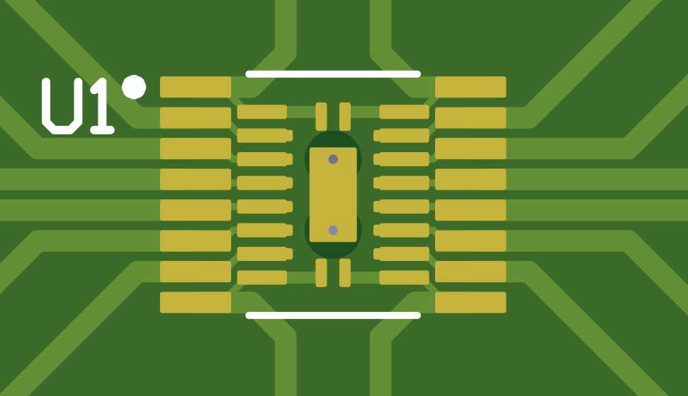
 Figure 5-1 DUT Footprint U1
The TMUXBQB-DYYEVM will not have any device connected at footprint U1, and there are not any devices included with the EVM for this footprint. Attach any compatible Texas Instruments TMUX device to this location, which will serve as the Device Under Test (DUT). Compatible devices include 16-pin parts with PW, BQB or DYY package names.
The headers of the TMUXBQB-DYYEVM can be easily connected to a power rail using 2.54 mm shunts on J1-J16, not included with the board. Connecting the shunt between pin 4 of the header and pin 3 (GND) to connect the corresponding pin of U1 to GND. Alternatively, the pins of U1 can be shorted to VDD or VSS by connecting between pin 4 of the header and pin 2 or pin 6 respectively. Figure 4-2 and Table 4-1 includes detailed descriptions of the connections on J1 through J16.
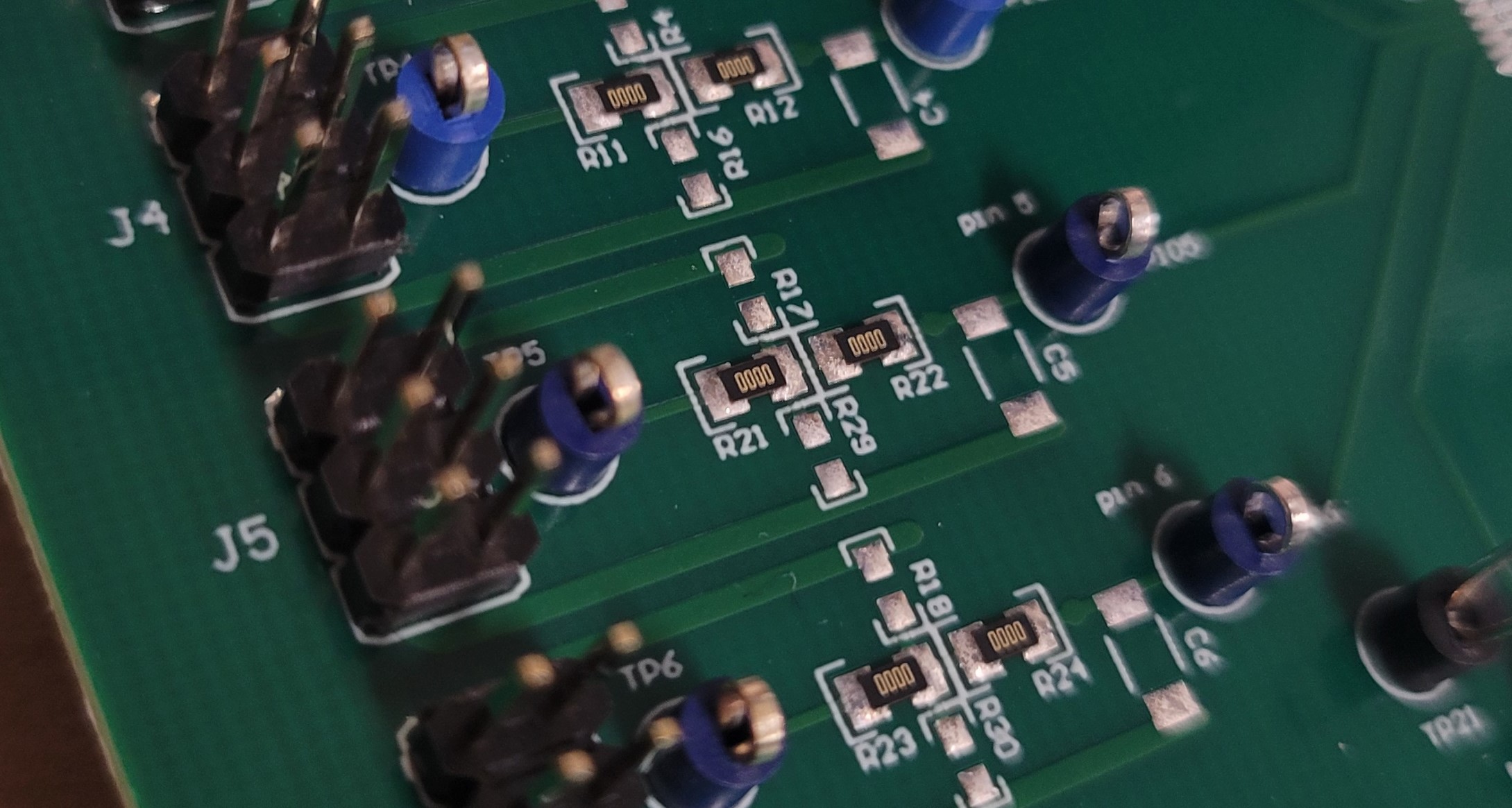
 Figure 5-2 Signal Line Circuitry (3D)
As shown in Figure 5-2 and Figure 5-3 as R21 and R22 on the J5 (pin 5 of U1) signal line, the TMUXBQB-DYYEVM includes 0 Ω series resistors (0805 package) on each signal line.
 Figure 5-3 Signal Line Circuitry
These can be substituted for different resistors as desired. Additionally, there are pads for pull-up and pull-down resistors to VDD and GND respectively. Add any 0603 resistor to the footprint shown as R17 to provide pull-up to VDD, and add any 0603 resistor to the footprint shown as R29 to provide pull-down to GND.
Each signal line also includes two footprints that allow for the user to attach capacitors or other devices with matching footprints. On the top side of the board, shown in Figure 5-2 and Figure 5-3 as C5, a standard 1206 footprint exists between the U1 pin signal and the GND signal. The user can solder a capacitor to this footprint to provide capacitance to the signal line.
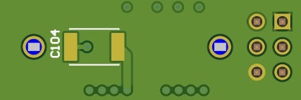
 Figure 5-4 Signal Line Circuitry Bottom Layer
On the back side of the board, shown in Figure 5-4 as C104, a standard 1812 footprint exists, also allowing for connection of a capacitor between the U1 pin signal and GND. The user can solder a capacitor to this footprint to provide capacitance to the signal line.