SCEU014B October 2018 – September 2022 SN74HCS74-Q1
2.2 Hardware Setup
This section will cover the six steps to take when evaluating a leaded Logic device using this EVM.
- Identify the package you will be using for the device being evaluated. As stated previously, this EVM has six sections each of which contains a footprint in which a logic device can be placed. Break off the selected section (optional).
- Solder down the device. Some sections support multiple packages, so carefully solder down the device to make sure it is aligned properly. If a device with less than 24 pins is being evaluated, then it should be placed towards the top of the footprint.
- Ensure the VCC pin of the device is
connected to the bypass capacitor. If pin 1 of the device is connected to pin 1
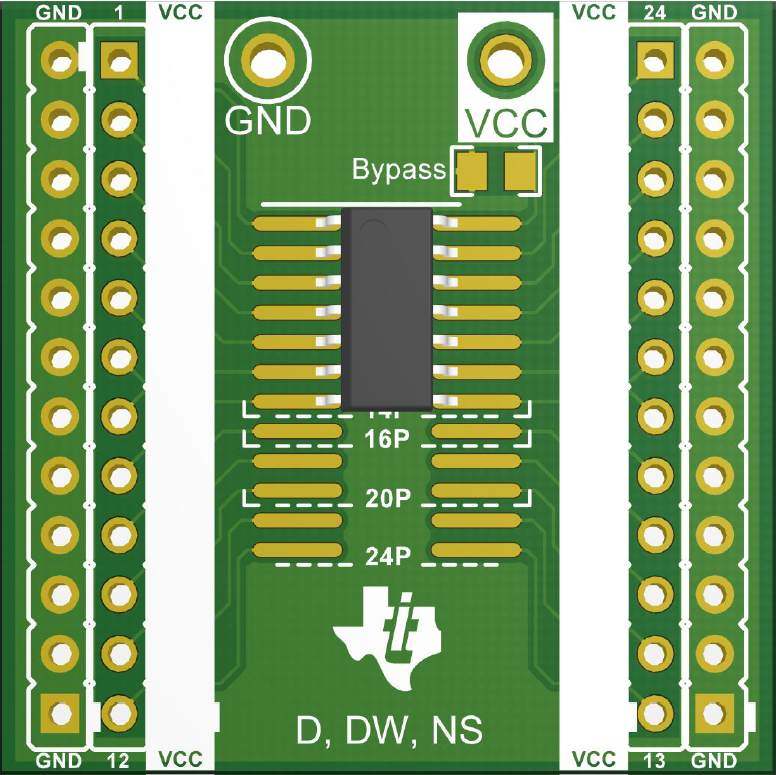
of the footprint, then it will be connected correctly. Figure 2-2 shows an example of a 14-pin device in the D package placed correctly on the
EVM.
 Figure 2-2 14-Pin Device in D
Package
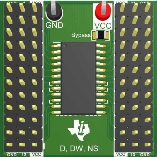
 - Interface with device pins. The kit includes six 12-pin headers which will allow the user to fully populate a single section. An example of this, with the addition of test points and a bypass capacitor for the supply, can be seen in Figure 2-3.
 Figure 2-3 Fully Populated Section
 - The device VCC pin will need to be connected to the VCC of the EVM. If using the headers, this can be accomplished using a simple shunt. If the headers are not being used then a simple solder bridge can be formed from the I/O header pad to the VCC header pad.
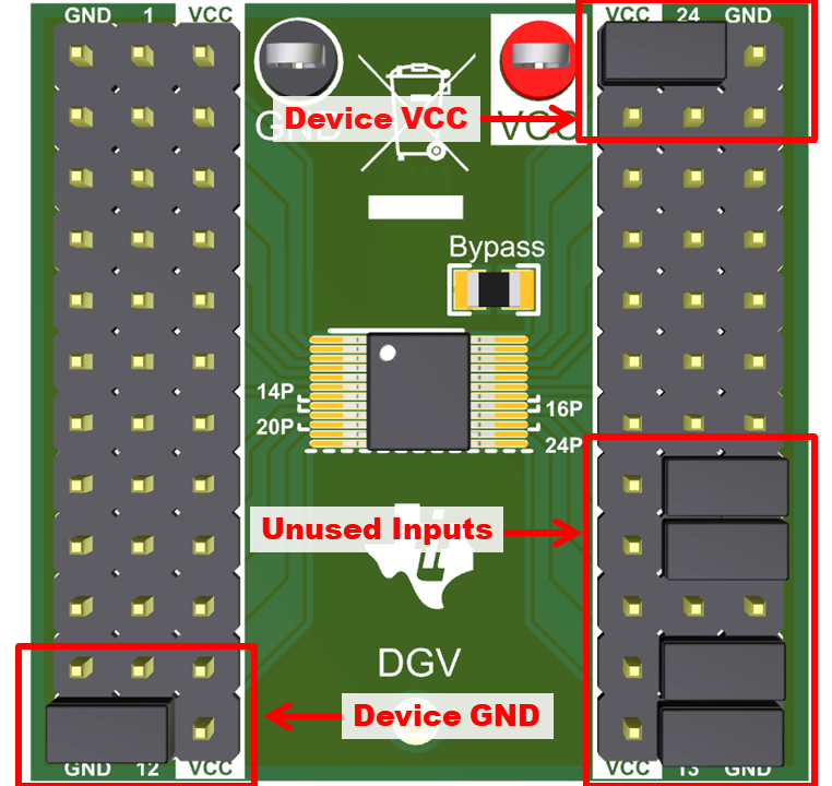
- Repeat step 5 for the GND pin and any unused input pins of the device. Figure 2-4 shows an example of how to use shunts to both power the device and tie unused inputs to a defined logic state to prevent them from floating. For more information on why it is important to avoid floating inputs, see the Implications of Slow or Floating CMOS Inputs application report.
 Figure 2-4 Shunt Usage for Device Evaluation
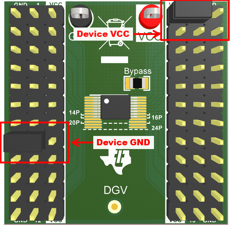
 Figure 2-5 Shunt Usage for 16-pin Device
Figure 2-5 shows that the GND shunt will shift up as the device pin count decreases even though the VCC will always be shunted in the top right assuming the device is placed correctly.