SLAA904C August 2019 – March 2020 MSP430FR2310 , MSP430FR2311 , MSP430FR2353 , MSP430FR2355
Design Goals
| Temperature | Output Voltage | Supply | ||||
|---|---|---|---|---|---|---|
| TMin | TMax | VoutMin | VoutMax | Vcc | Vee | Vref |
| 25℃ | 50℃ | 0.2 V | 3.1 V | 3.3 V | 0 V | 1.65 V |
Design Description
Some MSP430™ microcontrollers (MCUs) contain configurable integrated signal chain elements such as op-amps, DACs, and programmable gain stages. These elements make up a peripheral called the Smart Analog Combo (SAC). For information on the different types of SACs and how to leverage their configurable analog signal chain capabilities, visit MSP430 MCUs Smart Analog Combo Training. To get started with your design, download the Temperature Sensing NTC Circuit Design Files.
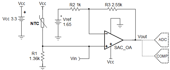
This temperature sensing circuit uses a resistor in series with a negative-temperature-coefficient (NTC) thermistor to form a voltage divider, which produces an output voltage that is linear over temperature. The circuit uses the MSP430FR2311 SAC_L1 op-amp in a noninverting amplifier configuration with inverting reference to offset and gain the signal, which helps to use the full ADC resolution and increase measurement accuracy. (Note: The MSP430FR2355 features four SAC_L3 peripherals which each contain a built-in DAC and PGA, providing a single-chip solution for generating Vref and measuring the thermistor circuit.) The output of the integrated SAC op-amp can be sampled directly by the on-board ADC or monitored by the on-board comparator for further processing inside the MCU.
Design Notes
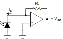
- The connection, Vin, is a negative temperature coefficient output voltage. To measure the output voltage of a PTC thermistor, switch the position of R1 and the thermistor.
- Vref can be generated using one of the integrated SAC_L3 DACs in the MSP430FR2355 or a voltage divider. If a voltage divider is used the equivalent resistance of the voltage divider will influence the gain of the circuit.
- Using high value resistors can degrade the phase margin of the amplifier and introduce additional noise in the circuit. It is recommended to use resistor values of approximately 10 kΩ or less.
- If the solution is implemented using the MSP430FR2311, the SAC_L1 op-amp is configured in general purpose mode to measure the thermistor circuit.
- If the solution is implemented using the MSP430FR2355, one SAC_L3 peripheral is configured in DAC mode to generate the reference voltage and another is configured in general purpose mode to measure the thermistor circuit.
Design Steps
- Calculate the value of R1 to produce a linear output voltage. Use the minimum and maximum values of the NTC to obtain a range of values for R1.
- Calculate the input voltage range.
- Calculate the gain required to produce the maximum output swing.
- Select R2 and calculate R3 to set the gain in Step 3.
- Calculate the actual gain based on standard values of R2 and R3.
- Calculate the output voltage swing based on the actual gain.
- Calculate the maximum output voltage when the output voltage is symmetrical around mid-supply.
- Calculate the reference voltage.
Design Simulations
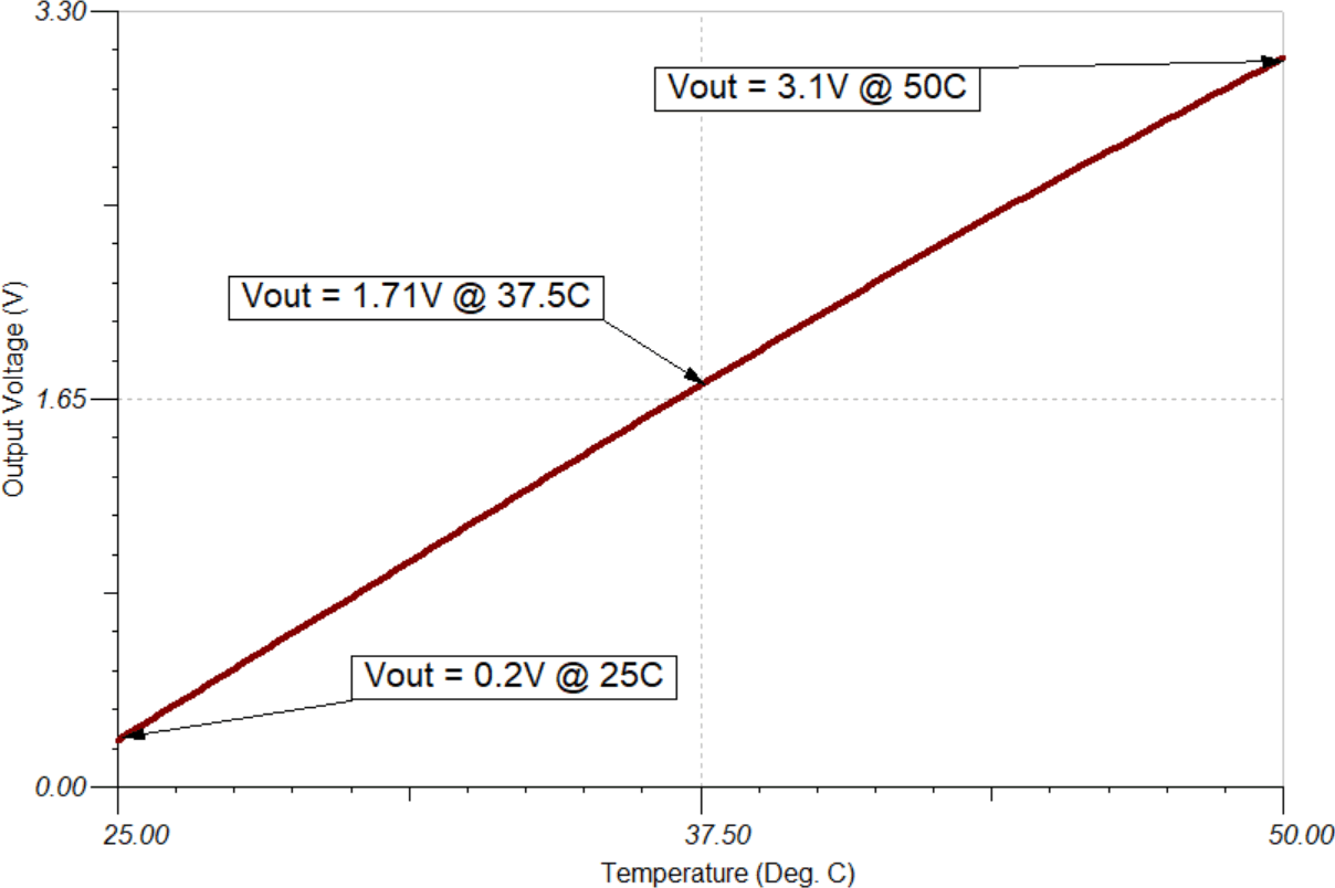
DC Transfer Results
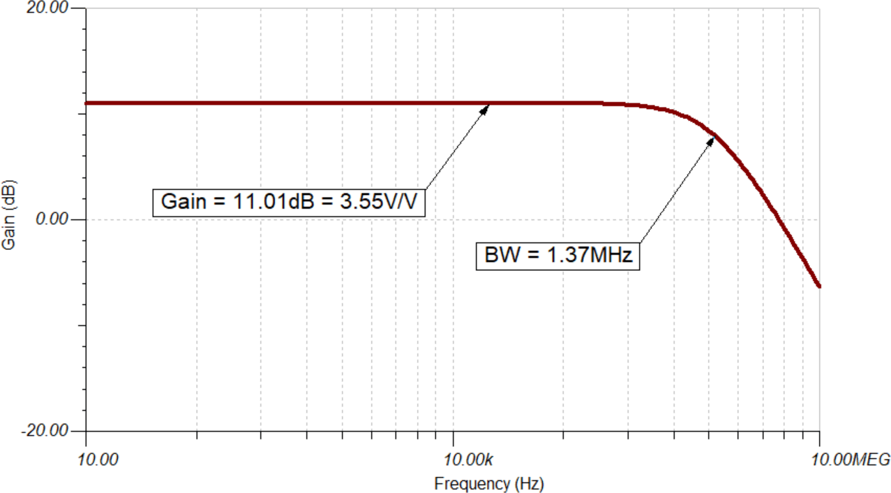
AC Simulation Results
Target Applications
- Field temperature transmitters
- Thermostats
- Thermometers
- Thermistor probes
- System temperature monitor
References
- MSP430 MCUs Smart Analog Combo Training
- Analog Engineer's Circuit Cookbooks
- MSP430FR2311 TINA-TI Spice Model
- MSP430 Temp Sense NTC Circuit Code Examples and SPICE Simulation File
Design Featured Op Amp
| MSP430FRxx Smart Analog Combo | ||
|---|---|---|
| MSP430FR2311 SAC_L1 | MSP430FR2355 SAC_L3 | |
| Vcc | 2.0 V to 3.6 V | |
| VCM | -0.1 V to VCC + 0.1 V | |
| Vout | Rail-to-rail | |
| Vos | ±5 mV | |
| AOL | 100 dB | |
| Iq | 350 µA (high-speed mode) | |
| 120 µA (low-power mode) | ||
| Ib | 50 pA | |
| UGBW | 4 MHz (high-speed mode) | 2.8 MHz (high-speed mode) |
| 1.4 MHz (low-power mode) | 1 MHz (low-power mode) | |
| SR | 3 V/µs (high-speed mode) | |
| 1 V/µs (low-power mode) | ||
| Number of channels | 1 | 4 |
| http://www.ti.com/product/MSP430FR2311 | ||
| http://www.ti.com/product/MSP430FR2355 | ||
Design Alternate Op Amp
| MSP430FR2311 Transimpedance Amplifier | |
|---|---|
| Vcc | 2.0 V to 3.6 V |
| VCM | -0.1 V to VCC/2 V |
| Vout | Rail-to-rail |
| Vos | ±5 mV |
| AOL | 100 dB |
| Iq | 350 µA (high-speed mode) |
| 120 µA (low-power mode) | |
| Ib | 5 pA (TSSOP-16 with OA-dedicated pin input) |
| 50 pA (TSSOP-20 and VQFN-16) | |
| UGBW | 5 MHz (high-speed mode) |
| 1.8 MHz (low-power mode) | |
| SR | 4 V/µs (high-speed mode) |
| 1 V/µs (low-power mode) | |
| Number of channels | 1 |
| http://www.ti.com/product/MSP430FR2311 | |