SLAA918B November 2019 – March 2020 MSP430FR2310 , MSP430FR2311 , MSP430FR2353 , MSP430FR2355
Design Goals
| Input | Output | Supply | |||
|---|---|---|---|---|---|
| IiMin | IiMax | VoMin | VoMax | Vcc | Vee |
| 25 mA | 300 mA | 0.25 V | 3 V | 3.3 V | 0 V |
Design Description
Some MSP430™ microcontrollers (MCUs) contain configurable integrated signal chain elements such as op-amps, DACs, and programmable gain stages. These elements make up a peripheral called the smart analog combo (SAC). For information on the different types of SACs and how to leverage their configurable analog signal chain capabilities, visit MSP430 MCUs Smart Analog Combo Training. To get started with your design, download the High-Side Current Sensing Circuit Design Files.
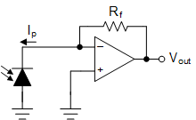
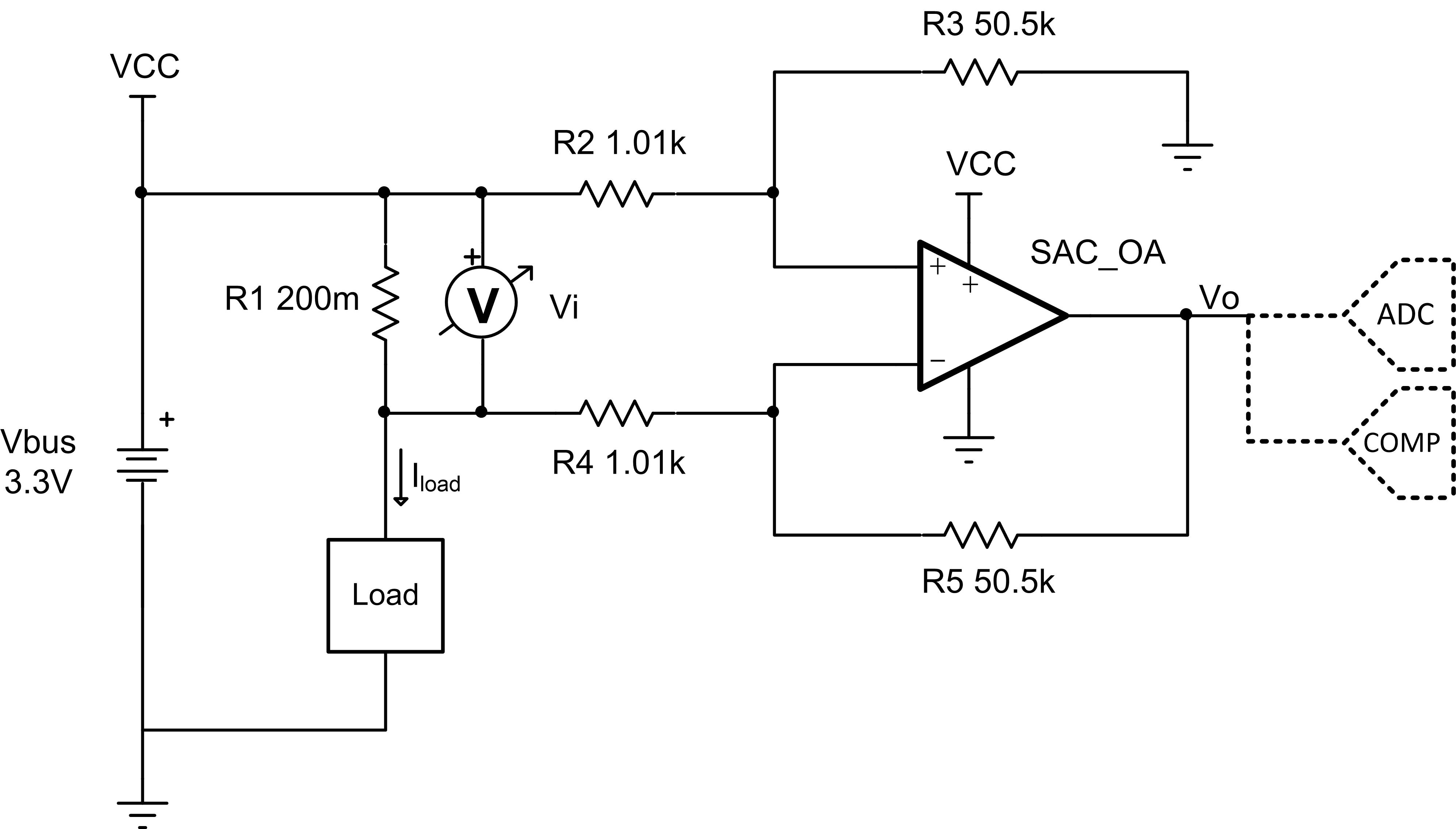
This single-supply, high-side, low-cost current sensing solution detects load current between 25 mA and 300 mA and converts it to an output voltage from 0.25 V to 3 V. High-side sensing allows for the system to identify ground shorts and does not create a ground disturbance on the load. The circuit uses the MSP430FR2311 SAC_L1 op-amp in general-purpose (GP) mode with OAx+ and OAx- dedicated as noninverting and inverting inputs. The same approach can be implemented with the MSP430FR2355, featuring four SAC_L3 peripherals with additional built-in DAC and PGA capabilities. The output of the integrated SAC op-amp can be sampled directly by the on-board ADC or monitored by the on-board comparator for further processing inside the MCU.
Design Notes
- DC common-mode rejection ratio (CMRR) performance is dependent on the matching of the gain setting resistors, R2-R5.
- Increasing the shunt resistor increases power dissipation.
- Ensure that the common-mode voltage is within the linear input operating region of the amplifier. The common-mode voltage is set by the resistor divider formed by R2, R3, and the bus voltage. Depending on the common-mode voltage determined by the resistor divider a rail-to-rail input (RRI) amplifier may not be required for this application.
- An op amp that does not have a common-mode voltage range that extends to Vcc may be used in low-gain or an attenuating configuration.
- A capacitor placed in parallel with the feedback resistor will limit bandwidth, improve stability, and help reduce noise.
- Use the op amp in a linear output operating region. Linear output swing is usually specified under the AOL test conditions.
- If the solution is implemented with the MSP430FR2311 SAC_L1 or with the MSP430FR2355 SAC_L3, the op-amp is configured in general-purpose mode.
- If the solution is implemented using the MSP430FR2311 TIA, the input voltage range is limited to VCC/2, so the gain or range must be adjusted accordingly.
- The High-Side Current Sensing Circuit Design Files include code examples showing how to properly initialize the SAC peripherals.
Design Steps
- The full transfer function of the circuit is provided below.
- Calculate the maximum shunt resistance. Set the maximum voltage across the shunt to 60 mV.
- Calculate the gain to set the maximum output swing range.
- Calculate the gain setting resistors to set the gain calculated in step 3.
- Calculate the common-mode voltage of the amplifier to ensure linear operation.
- The upper cutoff frequency (fH) is set by the non-inverting gain (noise gain) of the circuit and the gain bandwidth (GBW) of the op amp.
Design Simulations
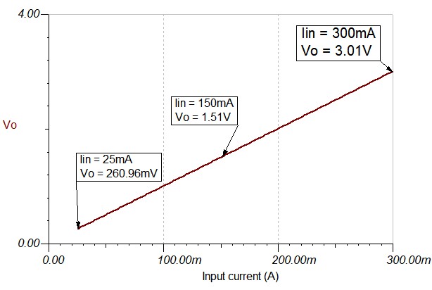
DC Simulation Results
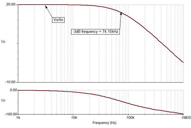
AC Simulation Results
Target Applications
- Cordless power tool battery pack
- E-bike, e-scooter battery pack
- Motor drives
- LED luminaire
- Grid infrastructure
References
- High-Side Current Sensing Circuit Design Files
- Analog Engineer's Circuit Cookbooks
- MSP430FR2311 TINA-TI Spice Model
- MSP430 MCUs Smart Analog Combo Training
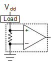
Design Featured Op Amp
| MSP430FRxx Smart Analog Combo | ||
|---|---|---|
| MSP430FR2311 SAC_L1 | MSP430FR2355 SAC_L3 | |
| Vcc | 2.0 V to 3.6 V | |
| VCM | -0.1 V to VCC + 0.1 V | |
| Vout | Rail-to-rail | |
| Vos | ±5 mV | |
| AOL | 100 dB | |
| Iq | 350 µA (high-speed mode) | |
| 120 µA (low-power mode) | ||
| Ib | 50 pA | |
| UGBW | 4 MHz (high-speed mode) | 2.8 MHz (high-speed mode) |
| 1.4 MHz (low-power mode) | 1 MHz (low-power mode) | |
| SR | 3 V/µs (high-speed mode) | |
| 1 V/µs (low-power mode) | ||
| Number of channels | 1 | 4 |
| http://www.ti.com/product/MSP430FR2311 | ||
| http://www.ti.com/product/MSP430FR2355 | ||
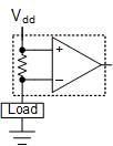
Design Alternate Op Amp
| MSP430FR2311 Transimpedance Amplifier | |
|---|---|
| Vcc | 2.0 V to 3.6 V |
| VCM | -0.1 V to VCC/2 V |
| Vout | Rail-to-rail |
| Vos | ±5 mV |
| AOL | 100 dB |
| Iq | 350 µA (high-speed mode) |
| 120 µA (low-power mode) | |
| Ib | 5 pA (TSSOP-16 with OA-dedicated pin input) |
| 50 pA (TSSOP-20 and VQFN-16) | |
| UGBW | 5 MHz (high-speed mode) |
| 1.8 MHz (low-power mode) | |
| SR | 4 V/µs (high-speed mode) |
| 1 V/µs (low-power mode) | |
| Number of channels | 1 |
| http://www.ti.com/product/MSP430FR2311 | |
Related MSP430 Circuits