SLAU144K December   2004  – August 2022 MSP430AFE221 , MSP430AFE222 , MSP430AFE223 , MSP430AFE231 , MSP430AFE232 , MSP430AFE233 , MSP430AFE251 , MSP430AFE252 , MSP430AFE253 , MSP430F2001 , MSP430F2002 , MSP430F2003 , MSP430F2011 , MSP430F2012 , MSP430F2013 , MSP430F2101 , MSP430F2111 , MSP430F2112 , MSP430F2121 , MSP430F2122 , MSP430F2131 , MSP430F2132 , MSP430F2132-EP , MSP430F2232 , MSP430F2234 , MSP430F2252 , MSP430F2252-Q1 , MSP430F2254 , MSP430F2272 , MSP430F2272-Q1 , MSP430F2274 , MSP430F2274-EP , MSP430F233 , MSP430F2330 , MSP430F235 , MSP430F2350 , MSP430F2370 , MSP430F2410 , MSP430F2416 , MSP430F2417 , MSP430F2418 , MSP430F2419 , MSP430F247 , MSP430F2471 , MSP430F248 , MSP430F2481 , MSP430F249 , MSP430F2491 , MSP430F2616 , MSP430F2617 , MSP430F2618 , MSP430F2619 , MSP430G2001 , MSP430G2101 , MSP430G2102 , MSP430G2111 , MSP430G2112 , MSP430G2121 , MSP430G2131 , MSP430G2132 , MSP430G2152 , MSP430G2153 , MSP430G2201 , MSP430G2201-Q1 , MSP430G2202 , MSP430G2203 , MSP430G2210 , MSP430G2211 , MSP430G2212 , MSP430G2213 , MSP430G2221 , MSP430G2230 , MSP430G2231 , MSP430G2231-Q1 , MSP430G2232 , MSP430G2233 , MSP430G2252 , MSP430G2253 , MSP430G2302 , MSP430G2303 , MSP430G2312 , MSP430G2313 , MSP430G2332 , MSP430G2333 , MSP430G2352 , MSP430G2353 , MSP430G2402 , MSP430G2403 , MSP430G2412 , MSP430G2413 , MSP430G2432 , MSP430G2433 , MSP430G2444 , MSP430G2452 , MSP430G2453 , MSP430G2513 , MSP430G2533 , MSP430G2544 , MSP430G2553 , MSP430G2744 , MSP430G2755 , MSP430G2855 , MSP430G2955 , MSP430TCH5E


  1.   Read This First
    1.     About This Manual
    2.     Related Documentation From Texas Instruments
    3.     Notational Conventions
    4.     Glossary
    5.     Register Bit Conventions
  2. Introduction
    1. 1.1 Architecture
    2. 1.2 Flexible Clock System
    3. 1.3 Embedded Emulation
    4. 1.4 Address Space
      1. 1.4.1 Flash/ROM
      2. 1.4.2 RAM
      3. 1.4.3 Peripheral Modules
      4. 1.4.4 Special Function Registers (SFRs)
      5. 1.4.5 Memory Organization
    5. 1.5 MSP430x2xx Family Enhancements
  3. System Resets, Interrupts, and Operating Modes
    1. 2.1 System Reset and Initialization
      1. 2.1.1 Brownout Reset (BOR)
      2. 2.1.2 Device Initial Conditions After System Reset
        1. 2.1.2.1 Software Initialization
    2. 2.2 Interrupts
      1. 2.2.1 (Non)-Maskable Interrupts (NMI)
        1. 2.2.1.1 Reset/NMI Pin
        2. 2.2.1.2 Flash Access Violation
        3. 2.2.1.3 Oscillator Fault
        4. 2.2.1.4 Example of an NMI Interrupt Handler
      2. 2.2.2 Maskable Interrupts
      3. 2.2.3 Interrupt Processing
        1. 2.2.3.1 Interrupt Acceptance
        2. 2.2.3.2 Return From Interrupt
        3. 2.2.3.3 Interrupt Nesting
      4. 2.2.4 Interrupt Vectors
    3. 2.3 Operating Modes
      1. 2.3.1 Entering and Exiting Low-Power Modes
    4. 2.4 Principles for Low-Power Applications
    5. 2.5 Connection of Unused Pins
  4. CPU
    1. 3.1 CPU Introduction
    2. 3.2 CPU Registers
      1. 3.2.1 Program Counter (PC)
      2. 3.2.2 Stack Pointer (SP)
      3. 3.2.3 Status Register (SR)
      4. 3.2.4 Constant Generator Registers CG1 and CG2
        1. 3.2.4.1 Constant Generator - Expanded Instruction Set
      5. 3.2.5 General-Purpose Registers R4 to R15
    3. 3.3 Addressing Modes
      1. 3.3.1 Register Mode
      2. 3.3.2 Indexed Mode
      3. 3.3.3 Symbolic Mode
      4. 3.3.4 Absolute Mode
      5. 3.3.5 Indirect Register Mode
      6. 3.3.6 Indirect Autoincrement Mode
      7. 3.3.7 Immediate Mode
    4. 3.4 Instruction Set
      1. 3.4.1 Double-Operand (Format I) Instructions
      2. 3.4.2 Single-Operand (Format II) Instructions
      3. 3.4.3 Jumps
      4. 3.4.4 Instruction Cycles and Lengths
        1. 3.4.4.1 Interrupt and Reset Cycles
        2. 3.4.4.2 Format-II (Single Operand) Instruction Cycles and Lengths
        3. 3.4.4.3 Format-III (Jump) Instruction Cycles and Lengths
        4. 3.4.4.4 Format-I (Double Operand) Instruction Cycles and Lengths
      5. 3.4.5 Instruction Set Description
      6. 3.4.6 Instruction Set Details
        1. 3.4.6.1  ADC
          1.        68
        2. 3.4.6.2  ADD
          1.        70
        3. 3.4.6.3  ADDC
          1.        72
        4. 3.4.6.4  AND
          1.        74
        5. 3.4.6.5  BIC
          1.        76
        6. 3.4.6.6  BIS
          1.        78
        7. 3.4.6.7  BIT
          1.        80
        8. 3.4.6.8  BR, BRANCH
          1.        82
        9. 3.4.6.9  CALL
          1.        84
        10. 3.4.6.10 CLR
          1.        86
        11. 3.4.6.11 CLRC
          1.        88
        12. 3.4.6.12 CLRN
          1.        90
        13. 3.4.6.13 CLRZ
          1.        92
        14. 3.4.6.14 CMP
          1.        94
        15. 3.4.6.15 DADC
          1.        96
        16. 3.4.6.16 DADD
          1.        98
        17. 3.4.6.17 DEC
          1.        100
        18. 3.4.6.18 DECD
          1.        102
        19. 3.4.6.19 DINT
          1.        104
        20. 3.4.6.20 EINT
          1.        106
        21. 3.4.6.21 INC
          1.        108
        22. 3.4.6.22 INCD
          1.        110
        23. 3.4.6.23 INV
          1.        112
        24. 3.4.6.24 JC, JHS
          1.        114
        25. 3.4.6.25 JEQ, JZ
          1.        116
        26. 3.4.6.26 JGE
          1.        118
        27. 3.4.6.27 JL
          1.        120
        28. 3.4.6.28 JMP
          1.        122
        29. 3.4.6.29 JN
          1.        124
        30. 3.4.6.30 JNC, JLO
          1.        126
        31. 3.4.6.31 JNE, JNZ
          1.        128
        32. 3.4.6.32 MOV
          1.        130
        33. 3.4.6.33 NOP
          1.        132
        34. 3.4.6.34 POP
          1.        134
        35. 3.4.6.35 PUSH
          1.        136
        36. 3.4.6.36 RET
          1.        138
        37. 3.4.6.37 RETI
          1.        140
        38. 3.4.6.38 RLA
          1.        142
        39. 3.4.6.39 RLC
          1.        144
        40. 3.4.6.40 RRA
          1.        146
        41. 3.4.6.41 RRC
          1.        148
        42. 3.4.6.42 SBC
          1.        150
        43. 3.4.6.43 SETC
          1.        152
        44. 3.4.6.44 SETN
          1.        154
        45. 3.4.6.45 SETZ
          1.        156
        46. 3.4.6.46 SUB
          1.        158
        47. 3.4.6.47 SUBC, SBB
          1.        160
        48. 3.4.6.48 SWPB
          1.        162
        49. 3.4.6.49 SXT
          1.        164
        50. 3.4.6.50 TST
          1. 3.4.6.50.1 166
        51. 3.4.6.51 XOR
          1. 3.4.6.51.1 168
  5. CPUX
    1. 4.1 CPU Introduction
    2. 4.2 Interrupts
    3. 4.3 CPU Registers
      1. 4.3.1 Program Counter (PC)
      2. 4.3.2 Stack Pointer (SP)
      3. 4.3.3 Status Register (SR)
      4. 4.3.4 Constant Generator Registers (CG1 and CG2)
        1. 4.3.4.1 Constant Generator – Expanded Instruction Set
      5. 4.3.5 General-Purpose Registers (R4 to R15)
    4. 4.4 Addressing Modes
      1. 4.4.1 Register Mode
      2. 4.4.2 Indexed Mode
        1. 4.4.2.1 Indexed Mode in Lower 64-KB Memory
        2. 4.4.2.2 MSP430 Instruction With Indexed Mode in Upper Memory
        3. 4.4.2.3 MSP430X Instruction With Indexed Mode
      3. 4.4.3 Symbolic Mode
        1. 4.4.3.1 Symbolic Mode in Lower 64KB
        2. 4.4.3.2 MSP430 Instruction With Symbolic Mode in Upper Memory
        3. 4.4.3.3 MSP430X Instruction With Symbolic Mode
      4. 4.4.4 Absolute Mode
        1. 4.4.4.1 Absolute Mode in Lower 64KB
        2. 4.4.4.2 MSP430X Instruction With Absolute Mode
      5. 4.4.5 Indirect Register Mode
      6. 4.4.6 Indirect Autoincrement Mode
      7. 4.4.7 Immediate Mode
        1. 4.4.7.1 MSP430 Instructions With Immediate Mode
        2. 4.4.7.2 MSP430X Instructions With Immediate Mode
    5. 4.5 MSP430 and MSP430X Instructions
      1. 4.5.1 MSP430 Instructions
        1. 4.5.1.1 MSP430 Double-Operand (Format I) Instructions
        2. 4.5.1.2 MSP430 Single-Operand (Format II) Instructions
        3. 4.5.1.3 Jump Instructions
        4. 4.5.1.4 Emulated Instructions
        5. 4.5.1.5 MSP430 Instruction Execution
          1. 4.5.1.5.1 Instruction Cycles and Length for Interrupt, Reset, and Subroutines
          2. 4.5.1.5.2 Format II (Single-Operand) Instruction Cycles and Lengths
          3. 4.5.1.5.3 Jump Instructions Cycles and Lengths
          4. 4.5.1.5.4 Format I (Double-Operand) Instruction Cycles and Lengths
      2. 4.5.2 MSP430X Extended Instructions
        1. 4.5.2.1 Register Mode Extension Word
        2. 4.5.2.2 Non-Register Mode Extension Word
        3. 4.5.2.3 Extended Double-Operand (Format I) Instructions
        4. 4.5.2.4 Extended Single-Operand (Format II) Instructions
          1. 4.5.2.4.1 Extended Format II Instruction Format Exceptions
        5. 4.5.2.5 Extended Emulated Instructions
        6. 4.5.2.6 MSP430X Address Instructions
        7. 4.5.2.7 MSP430X Instruction Execution
          1. 4.5.2.7.1 MSP430X Format II (Single-Operand) Instruction Cycles and Lengths
          2. 4.5.2.7.2 MSP430X Format I (Double-Operand) Instruction Cycles and Lengths
          3. 4.5.2.7.3 MSP430X Address Instruction Cycles and Lengths
    6. 4.6 Instruction Set Description
      1. 4.6.1 Extended Instruction Binary Descriptions
      2. 4.6.2 MSP430 Instructions
        1. 4.6.2.1  ADC
        2. 4.6.2.2  ADD
        3. 4.6.2.3  ADDC
        4. 4.6.2.4  AND
        5. 4.6.2.5  BIC
        6. 4.6.2.6  BIS
        7. 4.6.2.7  BIT
        8. 4.6.2.8  BR, BRANCH
        9. 4.6.2.9  CALL
        10. 4.6.2.10 CLR
        11. 4.6.2.11 CLRC
        12. 4.6.2.12 CLRN
        13. 4.6.2.13 CLRZ
        14. 4.6.2.14 CMP
        15. 4.6.2.15 DADC
        16. 4.6.2.16 DADD
        17. 4.6.2.17 DEC
        18. 4.6.2.18 DECD
        19. 4.6.2.19 DINT
        20. 4.6.2.20 EINT
        21. 4.6.2.21 INC
        22. 4.6.2.22 INCD
        23. 4.6.2.23 INV
        24. 4.6.2.24 JC, JHS
        25. 4.6.2.25 JEQ, JZ
        26. 4.6.2.26 JGE
        27. 4.6.2.27 JL
        28. 4.6.2.28 JMP
        29. 4.6.2.29 JN
        30. 4.6.2.30 JNC, JLO
        31. 4.6.2.31 JNZ, JNE
        32. 4.6.2.32 MOV
        33. 4.6.2.33 NOP
        34. 4.6.2.34 POP
        35. 4.6.2.35 PUSH
        36. 4.6.2.36 RET
        37. 4.6.2.37 RETI
        38. 4.6.2.38 RLA
        39. 4.6.2.39 RLC
        40. 4.6.2.40 RRA
        41. 4.6.2.41 RRC
        42. 4.6.2.42 SBC
        43. 4.6.2.43 SETC
        44. 4.6.2.44 SETN
        45. 4.6.2.45 SETZ
        46. 4.6.2.46 SUB
        47. 4.6.2.47 SUBC
        48. 4.6.2.48 SWPB
        49. 4.6.2.49 SXT
        50. 4.6.2.50 TST
        51. 4.6.2.51 XOR
      3. 4.6.3 MSP430X Extended Instructions
        1. 4.6.3.1  ADCX
        2. 4.6.3.2  ADDX
        3. 4.6.3.3  ADDCX
        4. 4.6.3.4  ANDX
        5. 4.6.3.5  BICX
        6. 4.6.3.6  BISX
        7. 4.6.3.7  BITX
        8. 4.6.3.8  CLRX
        9. 4.6.3.9  CMPX
        10. 4.6.3.10 DADCX
        11. 4.6.3.11 DADDX
        12. 4.6.3.12 DECX
        13. 4.6.3.13 DECDX
        14. 4.6.3.14 INCX
        15. 4.6.3.15 INCDX
        16. 4.6.3.16 INVX
        17. 4.6.3.17 MOVX
        18. 4.6.3.18 POPM
        19. 4.6.3.19 PUSHM
        20. 4.6.3.20 POPX
        21. 4.6.3.21 PUSHX
        22. 4.6.3.22 RLAM
        23. 4.6.3.23 RLAX
        24. 4.6.3.24 RLCX
        25. 4.6.3.25 RRAM
        26. 4.6.3.26 RRAX
        27. 4.6.3.27 RRCM
        28. 4.6.3.28 RRCX
        29. 4.6.3.29 RRUM
        30. 4.6.3.30 RRUX
        31. 4.6.3.31 SBCX
        32. 4.6.3.32 SUBX
        33. 4.6.3.33 SUBCX
        34. 4.6.3.34 SWPBX
        35. 4.6.3.35 SXTX
        36. 4.6.3.36 TSTX
        37. 4.6.3.37 XORX
      4. 4.6.4 MSP430X Address Instructions
        1. 4.6.4.1  ADDA
        2. 4.6.4.2  BRA
        3. 4.6.4.3  CALLA
        4. 4.6.4.4  CLRA
        5. 4.6.4.5  CMPA
        6. 4.6.4.6  DECDA
        7. 4.6.4.7  INCDA
        8. 4.6.4.8  MOVA
        9. 4.6.4.9  RETA
        10. 4.6.4.10 TSTA
        11. 4.6.4.11 SUBA
  6. Basic Clock Module+
    1. 5.1 Basic Clock Module+ Introduction
    2. 5.2 Basic Clock Module+ Operation
      1. 5.2.1 Basic Clock Module+ Features for Low-Power Applications
      2. 5.2.2 Internal Very-Low-Power Low-Frequency Oscillator (VLO)
      3. 5.2.3 LFXT1 Oscillator
      4. 5.2.4 XT2 Oscillator
      5. 5.2.5 Digitally Controlled Oscillator (DCO)
        1. 5.2.5.1 Disabling the DCO
        2. 5.2.5.2 Adjusting the DCO Frequency
        3. 5.2.5.3 Using an External Resistor (ROSC) for the DCO
      6. 5.2.6 DCO Modulator
      7. 5.2.7 Basic Clock Module+ Fail-Safe Operation
        1. 5.2.7.1 Sourcing MCLK from a Crystal
      8. 5.2.8 Synchronization of Clock Signals
    3. 5.3 Basic Clock Module+ Registers
  7. DMA Controller
    1. 6.1 DMA Introduction
    2. 6.2 DMA Operation
      1. 6.2.1  DMA Addressing Modes
      2. 6.2.2  DMA Transfer Modes
        1. 6.2.2.1 Single Transfer
        2. 6.2.2.2 Block Transfers
        3. 6.2.2.3 Burst-Block Transfers
      3. 6.2.3  Initiating DMA Transfers
        1. 6.2.3.1 Edge-Sensitive Triggers
        2. 6.2.3.2 Level-Sensitive Triggers
        3. 6.2.3.3 Halting Executing Instructions for DMA Transfers
      4. 6.2.4  Stopping DMA Transfers
      5. 6.2.5  DMA Channel Priorities
      6. 6.2.6  DMA Transfer Cycle Time
      7. 6.2.7  Using DMA With System Interrupts
      8. 6.2.8  DMA Controller Interrupts
        1. 6.2.8.1 DMAIV Software Example
      9. 6.2.9  Using the USCI_B I2C Module with the DMA Controller
      10. 6.2.10 Using ADC12 with the DMA Controller
      11. 6.2.11 Using DAC12 With the DMA Controller
      12. 6.2.12 Writing to Flash With the DMA Controller
    3. 6.3 DMA Registers
  8. Flash Memory Controller
    1. 7.1 Flash Memory Introduction
    2. 7.2 Flash Memory Segmentation
      1. 7.2.1 Segment A
    3. 7.3 Flash Memory Operation
      1. 7.3.1 Flash Memory Timing Generator
        1. 7.3.1.1 Flash Timing Generator Clock Selection
      2. 7.3.2 Erasing Flash Memory
        1. 7.3.2.1 Initiating an Erase From Within Flash Memory
        2. 7.3.2.2 Initiating an Erase From RAM
      3. 7.3.3 Writing Flash Memory
        1. 7.3.3.1 Byte or Word Write
        2. 7.3.3.2 Initiating a Byte or Word Write From Within Flash Memory
        3. 7.3.3.3 Initiating a Byte or Word Write From RAM
        4. 7.3.3.4 Block Write
        5. 7.3.3.5 Block Write Flow and Example
      4. 7.3.4 Flash Memory Access During Write or Erase
      5. 7.3.5 Stopping a Write or Erase Cycle
      6. 7.3.6 Marginal Read Mode
      7. 7.3.7 Configuring and Accessing the Flash Memory Controller
      8. 7.3.8 Flash Memory Controller Interrupts
      9. 7.3.9 Programming Flash Memory Devices
        1. 7.3.9.1 Programming Flash Memory With JTAG
        2. 7.3.9.2 Programming Flash Memory With the Bootloader (BSL)
        3. 7.3.9.3 Programming Flash Memory With a Custom Solution
    4. 7.4 Flash Registers
  9. Digital I/O
    1. 8.1 Digital I/O Introduction
    2. 8.2 Digital I/O Operation
      1. 8.2.1 Input Register PxIN
      2. 8.2.2 Output Registers PxOUT
      3. 8.2.3 Direction Registers PxDIR
      4. 8.2.4 Pullup or Pulldown Resistor Enable Registers PxREN
      5. 8.2.5 Function Select Registers PxSEL and PxSEL2
      6. 8.2.6 Pin Oscillator
      7. 8.2.7 P1 and P2 Interrupts
        1. 8.2.7.1 Interrupt Flag Registers P1IFG, P2IFG
        2. 8.2.7.2 Interrupt Edge Select Registers P1IES, P2IES
        3. 8.2.7.3 Interrupt Enable P1IE, P2IE
      8. 8.2.8 Configuring Unused Port Pins
    3. 8.3 Digital I/O Registers
      1. 8.3.1 PxIN Register
      2. 8.3.2 PxOUT Register
      3. 8.3.3 PxDIR Register
      4. 8.3.4 PxIFG Register
      5. 8.3.5 PxIES Register
      6. 8.3.6 PxIE Register
      7. 8.3.7 PxSEL Register
      8. 8.3.8 PxSEL2 Register
      9. 8.3.9 PxREN Register
  10. Supply Voltage Supervisor (SVS)
    1. 9.1 Supply Voltage Supervisor (SVS) Introduction
    2. 9.2 SVS Operation
      1. 9.2.1 Configuring the SVS
      2. 9.2.2 SVS Comparator Operation
      3. 9.2.3 Changing the VLDx Bits
      4. 9.2.4 SVS Operating Range
    3. 9.3 SVS Registers
  11. 10Watchdog Timer+ (WDT+)
    1. 10.1 Watchdog Timer+ (WDT+) Introduction
    2. 10.2 Watchdog Timer+ Operation
      1. 10.2.1 Watchdog Timer+ Counter
      2. 10.2.2 Watchdog Mode
      3. 10.2.3 Interval Timer Mode
      4. 10.2.4 Watchdog Timer+ Interrupts
      5. 10.2.5 Watchdog Timer+ Clock Fail-Safe Operation
      6. 10.2.6 Operation in Low-Power Modes
      7. 10.2.7 Software Examples
    3. 10.3 Watchdog Timer+ Registers
  12. 11Hardware Multiplier
    1. 11.1 Hardware Multiplier Introduction
    2. 11.2 Hardware Multiplier Operation
      1. 11.2.1 Operand Registers
      2. 11.2.2 Result Registers
        1. 11.2.2.1 MACS Underflow and Overflow
      3. 11.2.3 Software Examples
      4. 11.2.4 Indirect Addressing of RESLO
      5. 11.2.5 Using Interrupts
    3. 11.3 Hardware Multiplier Registers
  13. 12Timer_A
    1. 12.1 Timer_A Introduction
    2. 12.2 Timer_A Operation
      1. 12.2.1 16-Bit Timer Counter
        1. 12.2.1.1 Clock Source Select and Divider
      2. 12.2.2 Starting the Timer
      3. 12.2.3 Timer Mode Control
        1. 12.2.3.1 Up Mode
        2. 12.2.3.2 Changing the Period Register TACCR0
        3. 12.2.3.3 Continuous Mode
        4. 12.2.3.4 Use of the Continuous Mode
        5. 12.2.3.5 Up/Down Mode
        6. 12.2.3.6 Changing the Period Register TACCR0
        7. 12.2.3.7 Use of the Up/Down Mode
      4. 12.2.4 Capture/Compare Blocks
        1. 12.2.4.1 Capture Initiated by Software
        2. 12.2.4.2 Compare Mode
      5. 12.2.5 Output Unit
        1. 12.2.5.1 Output Modes
        2. 12.2.5.2 Output Example — Timer in Up Mode
        3. 12.2.5.3 Output Example — Timer in Continuous Mode
        4. 12.2.5.4 Output Example — Timer in Up/Down Mode
      6. 12.2.6 Timer_A Interrupts
        1. 12.2.6.1 TACCR0 Interrupt
        2. 12.2.6.2 TAIV, Interrupt Vector Generator
        3. 12.2.6.3 TAIV Software Example
    3. 12.3 Timer_A Registers
  14. 13Timer_B
    1. 13.1 Timer_B Introduction
      1. 13.1.1 Similarities and Differences From Timer_A
    2. 13.2 Timer_B Operation
      1. 13.2.1 16-Bit Timer Counter
        1. 13.2.1.1 TBR Length
        2. 13.2.1.2 Clock Source Select and Divider
      2. 13.2.2 Starting the Timer
      3. 13.2.3 Timer Mode Control
        1. 13.2.3.1 Up Mode
        2. 13.2.3.2 Changing the Period Register TBCL0
        3. 13.2.3.3 Continuous Mode
        4. 13.2.3.4 Use of the Continuous Mode
        5. 13.2.3.5 Up/Down Mode
        6. 13.2.3.6 Changing the Value of Period Register TBCL0
        7. 13.2.3.7 Use of the Up/Down Mode
      4. 13.2.4 Capture/Compare Blocks
        1. 13.2.4.1 Capture Mode
          1. 13.2.4.1.1 Capture Initiated by Software
        2. 13.2.4.2 Compare Mode
          1. 13.2.4.2.1 Compare Latch TBCLx
          2. 13.2.4.2.2 Grouping Compare Latches
      5. 13.2.5 Output Unit
        1. 13.2.5.1 Output Modes
          1. 13.2.5.1.1 Output Example, Timer in Up Mode
          2. 13.2.5.1.2 Output Example, Timer in Continuous Mode
          3. 13.2.5.1.3 Output Example, Timer in Up/Down Mode
      6. 13.2.6 Timer_B Interrupts
        1. 13.2.6.1 TBCCR0 Interrupt Vector
        2. 13.2.6.2 TBIV, Interrupt Vector Generator
        3. 13.2.6.3 TBIV, Interrupt Handler Examples
          1. 13.2.6.3.1 Recommended Use of TBIV
    3. 13.3 Timer_B Registers
  15. 14Universal Serial Interface (USI)
    1. 14.1 USI Introduction
    2. 14.2 USI Operation
      1. 14.2.1 USI Initialization
      2. 14.2.2 USI Clock Generation
      3. 14.2.3 SPI Mode
        1. 14.2.3.1 SPI Master Mode
        2. 14.2.3.2 SPI Slave Mode
        3. 14.2.3.3 USISR Operation
        4. 14.2.3.4 SPI Interrupts
      4. 14.2.4 I2C Mode
        1. 14.2.4.1 I2C Master Mode
        2. 14.2.4.2 I2C Slave Mode
        3. 14.2.4.3 I2C Transmitter
        4. 14.2.4.4 I2C Receiver
        5. 14.2.4.5 START Condition
        6. 14.2.4.6 STOP Condition
        7. 14.2.4.7 Releasing SCL
        8. 14.2.4.8 Arbitration
        9. 14.2.4.9 I2C Interrupts
    3. 14.3 USI Registers
  16. 15Universal Serial Communication Interface, UART Mode
    1. 15.1 USCI Overview
    2. 15.2 USCI Introduction: UART Mode
    3. 15.3 USCI Operation: UART Mode
      1. 15.3.1  USCI Initialization and Reset
      2. 15.3.2  Character Format
      3. 15.3.3  Asynchronous Communication Formats
        1. 15.3.3.1 Idle-Line Multiprocessor Format
        2. 15.3.3.2 Transmitting an Idle Frame
        3. 15.3.3.3 Address-Bit Multiprocessor Format
        4. 15.3.3.4 Break Reception and Generation
      4. 15.3.4  Automatic Baud Rate Detection
        1. 15.3.4.1 Transmitting a Break/Synch Field
      5. 15.3.5  IrDA Encoding and Decoding
        1. 15.3.5.1 IrDA Encoding
        2. 15.3.5.2 IrDA Decoding
      6. 15.3.6  Automatic Error Detection
      7. 15.3.7  USCI Receive Enable
        1. 15.3.7.1 Receive Data Glitch Suppression
      8. 15.3.8  USCI Transmit Enable
      9. 15.3.9  UART Baud Rate Generation
        1. 15.3.9.1 Low-Frequency Baud Rate Generation
        2. 15.3.9.2 Oversampling Baud Rate Generation
      10. 15.3.10 Setting a Baud Rate
        1. 15.3.10.1 Low-Frequency Baud Rate Mode Setting
        2. 15.3.10.2 Oversampling Baud Rate Mode Setting
      11. 15.3.11 Transmit Bit Timing
        1. 15.3.11.1 Low-Frequency Baud Rate Mode Bit Timing
        2. 15.3.11.2 Oversampling Baud Rate Mode Bit Timing
      12. 15.3.12 Receive Bit Timing
      13. 15.3.13 Typical Baud Rates and Errors
      14. 15.3.14 Using the USCI Module in UART Mode with Low Power Modes
      15. 15.3.15 USCI Interrupts
        1. 15.3.15.1 USCI Transmit Interrupt Operation
        2. 15.3.15.2 USCI Receive Interrupt Operation
        3. 15.3.15.3 USCI Interrupt Usage
          1. 15.3.15.3.1 Shared Interrupt Vectors Software Example, Data Receive
          2.        560
          3. 15.3.15.3.2 Shared Interrupt Vectors Software Example, Data Transmit
    4. 15.4 USCI Registers: UART Mode
  17. 16Universal Serial Communication Interface, SPI Mode
    1. 16.1 USCI Overview
    2. 16.2 USCI Introduction: SPI Mode
    3. 16.3 USCI Operation: SPI Mode
      1. 16.3.1 USCI Initialization and Reset
      2. 16.3.2 Character Format
      3. 16.3.3 Master Mode
        1. 16.3.3.1 Four-Pin SPI Master Mode
      4. 16.3.4 Slave Mode
        1. 16.3.4.1 Four-Pin SPI Slave Mode
      5. 16.3.5 SPI Enable
        1. 16.3.5.1 Transmit Enable
        2. 16.3.5.2 Receive Enable
      6. 16.3.6 Serial Clock Control
        1. 16.3.6.1 Serial Clock Polarity and Phase
      7. 16.3.7 Using the SPI Mode With Low-Power Modes
      8. 16.3.8 SPI Interrupts
        1. 16.3.8.1 SPI Transmit Interrupt Operation
        2. 16.3.8.2 SPI Receive Interrupt Operation
        3. 16.3.8.3 USCI Interrupt Usage
          1. 16.3.8.3.1 Shared Receive Interrupt Vectors Software Example
          2.        584
          3. 16.3.8.3.2 Shared Transmit Interrupt Vectors Software Example
    4. 16.4 USCI Registers: SPI Mode
  18. 17Universal Serial Communication Interface, I2C Mode
    1. 17.1 USCI Overview
    2. 17.2 USCI Introduction: I2C Mode
    3. 17.3 USCI Operation: I2C Mode
      1. 17.3.1 USCI Initialization and Reset
      2. 17.3.2 I2C Serial Data
      3. 17.3.3 I2C Addressing Modes
        1. 17.3.3.1 7-Bit Addressing
        2. 17.3.3.2 10-Bit Addressing
        3. 17.3.3.3 Repeated Start Conditions
      4. 17.3.4 I2C Module Operating Modes
        1. 17.3.4.1 Slave Mode
          1. 17.3.4.1.1 I2C Slave Transmitter Mode
          2. 17.3.4.1.2 I2C Slave Receiver Mode
          3. 17.3.4.1.3 I2C Slave 10-bit Addressing Mode
        2. 17.3.4.2 Master Mode
          1. 17.3.4.2.1 I2C Master Transmitter Mode
          2. 17.3.4.2.2 I2C Master Receiver Mode
          3. 17.3.4.2.3 I2C Master 10-Bit Addressing Mode
          4. 17.3.4.2.4 Arbitration
      5. 17.3.5 I2C Clock Generation and Synchronization
        1. 17.3.5.1 Clock Stretching
      6. 17.3.6 Using the USCI Module in I2C Mode with Low-Power Modes
      7. 17.3.7 USCI Interrupts in I2C Mode
        1. 17.3.7.1 I2C Transmit Interrupt Operation
        2. 17.3.7.2 I2C Receive Interrupt Operation
        3. 17.3.7.3 I2C State Change Interrupt Operation
        4. 17.3.7.4 Interrupt Vector Assignment
          1. 17.3.7.4.1 Shared Receive Interrupt Vectors Software Example
          2.        616
          3. 17.3.7.4.2 Shared Transmit Interrupt Vectors Software Example
    4. 17.4 USCI Registers: I2C Mode
  19. 18USART Peripheral Interface, UART Mode
    1. 18.1 USART Introduction: UART Mode
    2. 18.2 USART Operation: UART Mode
      1. 18.2.1 USART Initialization and Reset
      2. 18.2.2 Character Format
      3. 18.2.3 Asynchronous Communication Formats
        1. 18.2.3.1 Idle-Line Multiprocessor Format
        2. 18.2.3.2 Address-Bit Multiprocessor Format
        3. 18.2.3.3 Automatic Error Detection
      4. 18.2.4 USART Receive Enable
      5. 18.2.5 USART Transmit Enable
      6. 18.2.6 USART Baud Rate Generation
        1. 18.2.6.1 Baud Rate Bit Timing
        2. 18.2.6.2 Determining the Modulation Value
        3. 18.2.6.3 Transmit Bit Timing
        4. 18.2.6.4 Receive Bit Timing
        5. 18.2.6.5 Typical Baud Rates and Errors
      7. 18.2.7 USART Interrupts
        1. 18.2.7.1 USART Transmit Interrupt Operation
        2. 18.2.7.2 USART Receive Interrupt Operation
        3. 18.2.7.3 Receive-Start Edge Detect Operation
        4. 18.2.7.4 Receive-Start Edge Detect Conditions
    3. 18.3 USART Registers – UART Mode
  20. 19USART Peripheral Interface, SPI Mode
    1. 19.1 USART Introduction: SPI Mode
    2. 19.2 USART Operation: SPI Mode
      1. 19.2.1 USART Initialization and Reset
      2. 19.2.2 Master Mode
        1. 19.2.2.1 Four-Pin SPI Master Mode
      3. 19.2.3 Slave Mode
        1. 19.2.3.1 Four-Pin SPI Slave Mode
      4. 19.2.4 SPI Enable
        1. 19.2.4.1 Transmit Enable
        2. 19.2.4.2 Receive Enable
      5. 19.2.5 Serial Clock Control
        1. 19.2.5.1 Serial Clock Polarity and Phase
      6. 19.2.6 SPI Interrupts
        1. 19.2.6.1 SPI Transmit Interrupt Operation
        2. 19.2.6.2 SPI Receive Interrupt Operation
    3. 19.3 USART Registers: SPI Mode
  21. 20OA
    1. 20.1 OA Introduction
    2. 20.2 OA Operation
      1. 20.2.1 OA Amplifier
      2. 20.2.2 OA Input
      3. 20.2.3 OA Output and Feedback Routing
      4. 20.2.4 OA Configurations
        1. 20.2.4.1 General Purpose Opamp Mode
        2. 20.2.4.2 Unity Gain Mode for Differential Amplifier
        3. 20.2.4.3 Unity Gain Mode
        4. 20.2.4.4 Comparator Mode
        5. 20.2.4.5 Non-Inverting PGA Mode
        6. 20.2.4.6 Cascaded Non-Inverting PGA Mode
        7. 20.2.4.7 Inverting PGA Mode
        8. 20.2.4.8 Differential Amplifier Mode
    3. 20.3 OA Registers
  22. 21Comparator_A+
    1. 21.1 Comparator_A+ Introduction
    2. 21.2 Comparator_A+ Operation
      1. 21.2.1 Comparator
      2. 21.2.2 Input Analog Switches
      3. 21.2.3 Input Short Switch
      4. 21.2.4 Output Filter
      5. 21.2.5 Voltage Reference Generator
      6. 21.2.6 Comparator_A+, Port Disable Register CAPD
      7. 21.2.7 Comparator_A+ Interrupts
      8. 21.2.8 Comparator_A+ Used to Measure Resistive Elements
    3. 21.3 Comparator_A+ Registers
  23. 22ADC10
    1. 22.1 ADC10 Introduction
    2. 22.2 ADC10 Operation
      1. 22.2.1  10-Bit ADC Core
        1. 22.2.1.1 Conversion Clock Selection
      2. 22.2.2  ADC10 Inputs and Multiplexer
        1. 22.2.2.1 Analog Port Selection
      3. 22.2.3  Voltage Reference Generator
        1. 22.2.3.1 Internal Reference Low-Power Features
      4. 22.2.4  Auto Power-Down
      5. 22.2.5  Sample and Conversion Timing
        1. 22.2.5.1 Sample Timing Considerations
      6. 22.2.6  Conversion Modes
        1. 22.2.6.1 Single-Channel Single-Conversion Mode
        2. 22.2.6.2 Sequence-of-Channels Mode
        3. 22.2.6.3 Repeat-Single-Channel Mode
        4. 22.2.6.4 Repeat-Sequence-of-Channels Mode
        5. 22.2.6.5 Using the MSC Bit
        6. 22.2.6.6 Stopping Conversions
      7. 22.2.7  ADC10 Data Transfer Controller
        1. 22.2.7.1 One-Block Transfer Mode
        2. 22.2.7.2 Two-Block Transfer Mode
        3. 22.2.7.3 Continuous Transfer
        4. 22.2.7.4 DTC Transfer Cycle Time
      8. 22.2.8  Using the Integrated Temperature Sensor
      9. 22.2.9  ADC10 Grounding and Noise Considerations
      10. 22.2.10 ADC10 Interrupts
    3. 22.3 ADC10 Registers
  24. 23ADC12
    1. 23.1 ADC12 Introduction
    2. 23.2 ADC12 Operation
      1. 23.2.1 12-Bit ADC Core
        1. 23.2.1.1 Conversion Clock Selection
      2. 23.2.2 ADC12 Inputs and Multiplexer
        1. 23.2.2.1 Analog Port Selection
      3. 23.2.3 Voltage Reference Generator
      4. 23.2.4 Sample and Conversion Timing
        1. 23.2.4.1 Extended Sample Mode
        2. 23.2.4.2 Pulse Sample Mode
        3. 23.2.4.3 Sample Timing Considerations
      5. 23.2.5 Conversion Memory
      6. 23.2.6 ADC12 Conversion Modes
        1. 23.2.6.1 Single-Channel Single-Conversion Mode
        2. 23.2.6.2 Sequence-of-Channels Mode
        3. 23.2.6.3 Repeat-Single-Channel Mode
        4. 23.2.6.4 Repeat-Sequence-of-Channels Mode
        5. 23.2.6.5 Using the Multiple Sample and Convert (MSC) Bit
        6. 23.2.6.6 Stopping Conversions
      7. 23.2.7 Using the Integrated Temperature Sensor
      8. 23.2.8 ADC12 Grounding and Noise Considerations
      9. 23.2.9 ADC12 Interrupts
        1. 23.2.9.1 ADC12IV, Interrupt Vector Generator
        2. 23.2.9.2 ADC12 Interrupt Handling Software Example
          1. 23.2.9.2.1 Interrupt Handling
    3. 23.3 ADC12 Registers
  25. 24TLV Structure
    1. 24.1 TLV Introduction
    2. 24.2 Supported Tags
      1. 24.2.1 DCO Calibration TLV Structure
        1. 24.2.1.1 Code Example Using Absolute Addressing Mode
        2.       747
        3. 24.2.1.2 Code Example Using the TLV Structure
      2. 24.2.2 TAG_ADC12_1 Calibration TLV Structure
        1. 24.2.2.1 Temperature Sensor Calibration Data
        2. 24.2.2.2 Integrated Voltage Reference Calibration Data
        3. 24.2.2.3 Example Using the Reference Calibration
        4. 24.2.2.4 Offset and Gain Calibration Data
        5. 24.2.2.5 Example Using Gain and Offset Calibration
    3. 24.3 Checking Integrity of SegmentA
    4. 24.4 Parsing TLV Structure of Segment A
  26. 25DAC12
    1. 25.1 DAC12 Introduction
    2. 25.2 DAC12 Operation
      1. 25.2.1 DAC12 Core
        1. 25.2.1.1 DAC12 Port Selection
      2. 25.2.2 DAC12 Reference
        1. 25.2.2.1 DAC12 Reference Input and Voltage Output Buffers
      3. 25.2.3 Updating the DAC12 Voltage Output
      4. 25.2.4 DAC12_xDAT Data Format
      5. 25.2.5 DAC12 Output Amplifier Offset Calibration
      6. 25.2.6 Grouping Multiple DAC12 Modules
      7. 25.2.7 DAC12 Interrupts
    3. 25.3 DAC12 Registers
  27. 26SD16_A
    1. 26.1 SD16_A Introduction
    2. 26.2 SD16_A Operation
      1. 26.2.1  ADC Core
      2. 26.2.2  Analog Input Range and PGA
      3. 26.2.3  Voltage Reference Generator
      4. 26.2.4  Auto Power-Down
      5. 26.2.5  Analog Input Pair Selection
        1. 26.2.5.1 Analog Input Setup
      6. 26.2.6  Analog Input Characteristics
      7. 26.2.7  Digital Filter
        1. 26.2.7.1 Digital Filter Output
      8. 26.2.8  Conversion Memory Register: SD16MEM0
        1. 26.2.8.1 Output Data Format
      9. 26.2.9  Conversion Modes
        1. 26.2.9.1 Single Conversion
        2. 26.2.9.2 Continuous Conversion
      10. 26.2.10 Using the Integrated Temperature Sensor
      11. 26.2.11 Interrupt Handling
        1. 26.2.11.1 SD16IV, Interrupt Vector Generator
        2. 26.2.11.2 Interrupt Delay Operation
    3. 26.3 SD16_A Registers
  28. 27SD24_A
    1. 27.1 SD24_A Introduction
    2. 27.2 SD24_A Operation
      1. 27.2.1  ADC Core
      2. 27.2.2  Analog Input Range and PGA
      3. 27.2.3  Voltage Reference Generator
      4. 27.2.4  Auto Power-Down
      5. 27.2.5  Analog Input Pair Selection
        1. 27.2.5.1 Analog Input Setup
      6. 27.2.6  Analog Input Characteristics
      7. 27.2.7  Digital Filter
        1. 27.2.7.1 Digital Filter Output
      8. 27.2.8  Conversion Memory Register: SD24MEMx
        1. 27.2.8.1 Output Data Format
      9. 27.2.9  Conversion Modes
        1. 27.2.9.1 Single Channel, Single Conversion
        2. 27.2.9.2 Single Channel, Continuous Conversion
        3. 27.2.9.3 Group of Channels, Single Conversion
        4. 27.2.9.4 Group of Channels, Continuous Conversion
      10. 27.2.10 Conversion Operation Using Preload
      11. 27.2.11 Using the Integrated Temperature Sensor
      12. 27.2.12 Interrupt Handling
        1. 27.2.12.1 SD24IV, Interrupt Vector Generator
        2. 27.2.12.2 Interrupt Delay Operation
        3. 27.2.12.3 SD24_A Interrupt Handling Software Example
    3. 27.3 SD24_A Registers
  29. 28Embedded Emulation Module (EEM)
    1. 28.1 EEM Introduction
    2. 28.2 EEM Building Blocks
      1. 28.2.1 Triggers
      2. 28.2.2 Trigger Sequencer
      3. 28.2.3 State Storage (Internal Trace Buffer)
      4. 28.2.4 Clock Control
    3. 28.3 EEM Configurations
  30.   Revision History

Low-Frequency Baud Rate Mode Bit Timing

In low-frequency mode, calculate the length of bit i Tbit,TX[i] based on the UCBRx and UCBRSx settings:
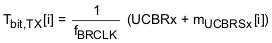
GUID-68068C02-3B37-4757-81EA-A09C8ABF63FD-low.gif

Where,

mUCBRSx[i] = Modulation of bit i from Table 15-2