SLLU346 April 2022 SN6507
6 EVM Schematic and PCB
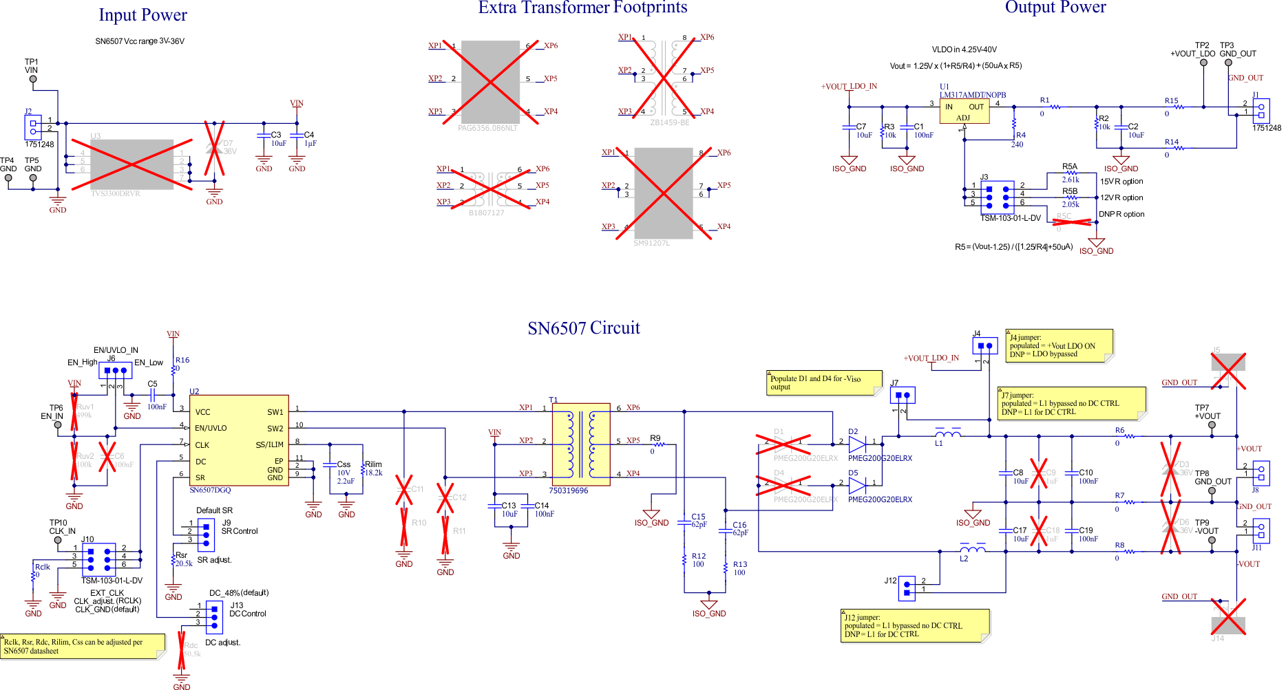
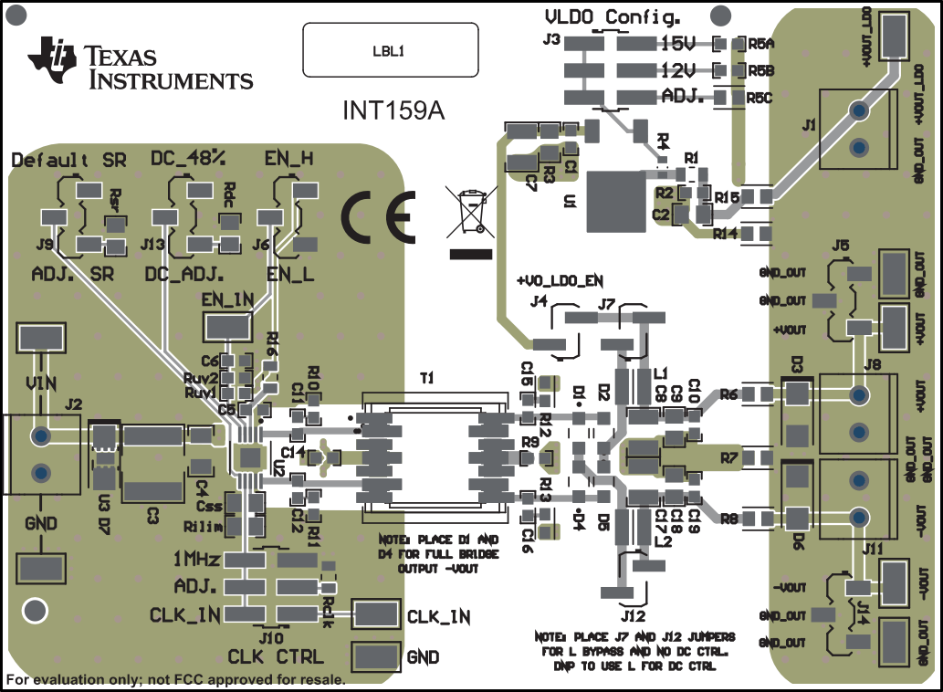
Figure 6-1 shows the schematic diagram for this EVM, and Figure 6-2 and Figure 6-3 show the printed circuit board (PCB) layout.
 Figure 6-1 SN6507DGQEVM Schematic
 Figure 6-2 SN6507DGQEVM Top PCB
Layout
 Figure 6-3 SN6507DGQEVM Bottom PCB
Layout