SLOA292 May 2020 TAS5760LD
4.2 Feedback Resistor Network Design and Simulation
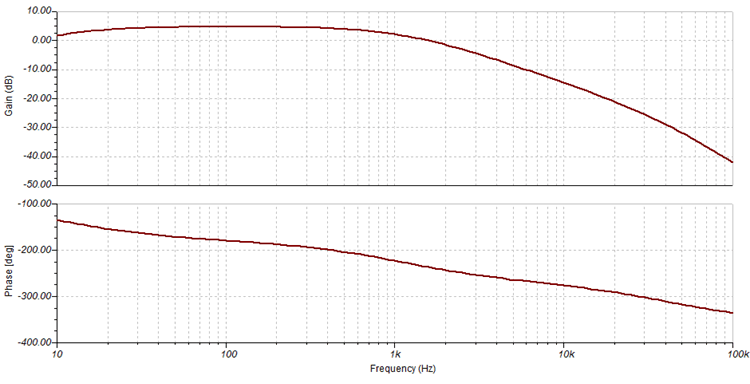
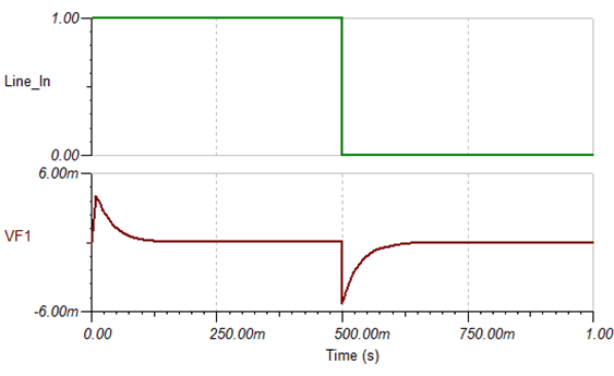
The design changes the feedback network resistor twice. The design feedback network resistors values are list in Table 2. From TINA’s simulation, the frequency response of Figure 11 stays flat from 20Hz to 200Hz. Step response simulation of Figure 12 shows that the VF1 (the Line driver output) transient can be improved from -6 mV to -2.5 mV.
Table 2. Design Parameters on the Feedback Network Resistors
| Parameter | Example |
|---|---|
| R1 | 24 kΩ |
| R2 | 24 kΩ |
| R3 | 7.5 kΩ |
| R4 | 56 kΩ |
| R5 | 270 Ω |
 Figure 10. Subwoofer Line Driver Stereo to Mono Design With Output Impedance 270Ω Resistor and Twice Feedback Network Resistor
  Figure 11. Frequency Response of Termination Resistor 270Ω. Increase the Feedback Resistor Values but Keep the Same Gain Level
  Figure 12. Step Responses With Termination Resistor 270 Ω. Increase the Feedback Resistor Values but Keep the Same Gain Level
 Replacing the 0 Ω resistor with the 47 nF high-pass capacitor can improve the transient from -6 mV to -1.6 mV. However, adding a high-pass capacitor also dramatically sacrifices the low-frequency response 20Hz to 200Hz. Therefore, using the high-pass capacitor at the line driver output is not suitable for the subwoofer line driver application