SLOA292 May 2020 TAS5760LD
5.2 Feedback Resistor Network Design With Practical Application Waveform
The circuit further increases the feedback gain resistor network value 2 times as shown in Table 2. The output transient is implicit due to the level is almost as same as the background noise.
Cons:
Equation 4. 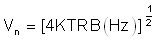
where, K = 1.38 × 10 23 J/K is Boltzmann’s constant, T is the absolute temperature (K), and B(Hz) is the bandwidth of the system.
Equation 5. 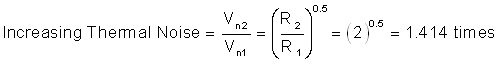
 Figure 14. Increasing Line Driver Feedback Resistor Network’s Waveform With 270Ω Termination Resistor
 CH1 is input from SOC. CH2 is line driver output. CH3 is (DR_MUTE)̅ controlled waveform by SOC’s GPIO. CH4 is 3.3V for line driver power.