SLUA963B June 2020 – October 2022 UCC21710-Q1 , UCC21732-Q1 , UCC5870-Q1
- HEV/EV Traction Inverter Design Guide Using Isolated IGBT and SiC Gate Drivers
- 1Introduction
- 2HEV/EV Overview
-
3Design of HEV/EV Traction Inverter Drive Stage
- 3.1 Introduction to UCC217xx-Q1
- 3.2 Designing a Traction Inverter Drive System Using UCC217xx-Q1
- 3.3 Description of Protection Features
- 3.4 Protection Features of UCC217xx-Q1
- 3.5
UCC217xx-Q1 Protection and Monitoring Features Descriptions
- 3.5.1 Primary and Secondary Side UVLO and OVLO
- 3.5.2 Over-Current (OC) and Desaturation (DESAT) Detection
- 3.5.3 2-Level and Soft Turn-Off
- 3.5.4 Power Switch Gate Voltage (VGE/VGS) Monitoring
- 3.5.5 Power Switch Anti-Shoot-Through
- 3.5.6 Integrated Internal or External Miller Clamp
- 3.5.7 Isolated Analog-to-PWM Channel
- 3.5.8 Short-Circuit Clamping
- 3.5.9 Active Pulldown
- 3.6 Introduction to UCC5870-Q1
- 3.7 Designing a Traction Inverter Drive System Using UCC5870-Q1
- 3.8 Description of Protection Features
- 3.9 Protection Features of UCC5870-Q1
- 3.10
UCC5870-Q1 Protection and Monitoring Features Descriptions
- 3.10.1 Primary and Secondary Side UVLO and OVLO
- 3.10.2 Programmable Desaturation (DESAT) Detection and Over-Current (OC)
- 3.10.3 Adjustable 2-Level or Soft Turn-Off
- 3.10.4 Active High-Voltage Clamp
- 3.10.5 Power Switch Gate Voltage (VGE/VGS) Monitoring
- 3.10.6 Gate Threshold Voltage Monitor
- 3.10.7 Power Switch Anti-Shoot-Through
- 3.10.8 Active Short Circuit (ASC)
- 3.10.9 Integrated Internal or External Miller Clamp
- 3.10.10 Isolated Analog-to-Digital Converter
- 3.10.11 Short-Circuit Clamping
- 3.10.12 Active and Passive Pulldown
- 3.10.13 Thermal Shutdown and Temperature Warning of Driver IC
- 3.10.14 Clock Monitor and CRC
- 3.10.15 SPI and Register Data Protection
- 4Isolated Bias Supply Architecture
- 5Summary
- 6References
- 7Revision History
3.10.2 Programmable Desaturation (DESAT) Detection and Over-Current (OC)
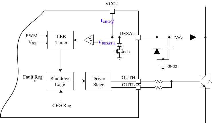
DESAT protection prevents the power transistor from damage in case of short circuit faults, which can be a result of incorrect control signals or a mechanical short. The DESAT input monitors the VCEsat (IGBT)/VDSon (MOSFET) through an external resistor and diode network, shown in Figure 3-17. The configuration of the DESAT pin is the same as the UCC21750-Q1. However, SPI programming enables the thresholds, blanking time, charging current, and deglitch filters to be programmable in order to best fit the system requirement. When a fault occurs, it will be indicated in a Status Register readable by the controller and can also trigger the nFLT1 output. The turn-off of the driver output during a DESAT fault is selectable between normal, soft turn-off (STO), or two-level turnoff (2LTO) as configured via SPI. The various configurations for DESAT allow for a high level of system optimization based on switch type and power level. This only enhances the level of protection and ability to mitigate failures.
 Figure 3-17 DESAT circuit configuration
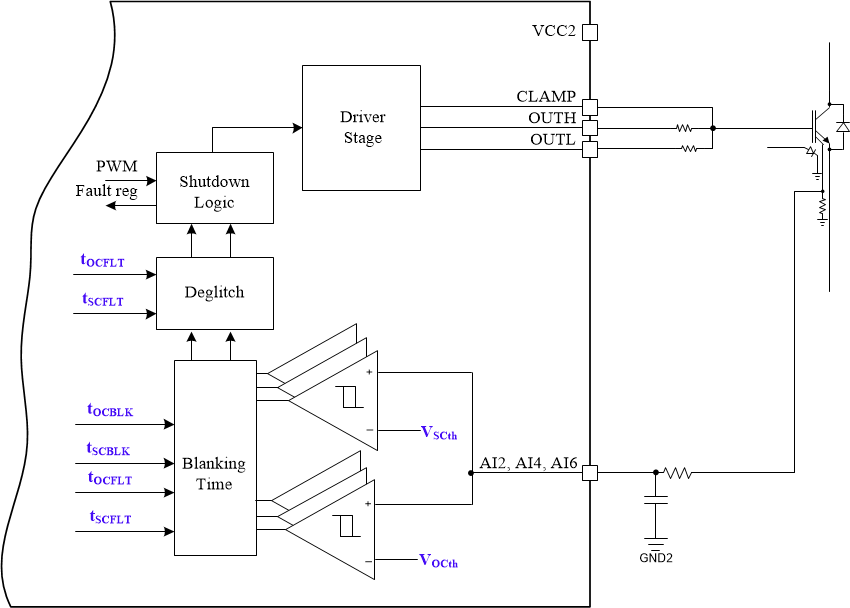
Overcurrent and short circuit protection (OCP and SCP) is supported via three AIx inputs (AI2, AI4, AI6) for shunt resistor based OCP and SCP, shown in Figure 3-18. Shunt resistor-based OCP/SCP protections are intended for power transistors with integrated current sense FETs, similar to the configuration that can be used with UCC21710-Q1 or UCC21732-Q1. The mirrored power transistor currents are fed into a resistor, and the voltage is monitored at the AIx input. Once the voltage at the AIx input exceeds the threshold programmed using the Configuration Registers, the fault is indicated in the Status Register. If unmasked, nFLTx is pulled low and the driver output goes to the state defined by the Configuration Registers; this can be configured as normal turn-off, STO, or 2LTO. A blanking time is used for both OCP and SCP to prevent unwanted false protection triggering during transitions and is also selectable. The thresholds for OCP and SCP, deglitch timing, blanking time, and reporting and driver action are all programmable via SPI.
 Figure 3-18 OC circuit configuration