SLUA963B June 2020 – October 2022 UCC21710-Q1 , UCC21732-Q1 , UCC5870-Q1
- HEV/EV Traction Inverter Design Guide Using Isolated IGBT and SiC Gate Drivers
- 1Introduction
- 2HEV/EV Overview
-
3Design of HEV/EV Traction Inverter Drive Stage
- 3.1 Introduction to UCC217xx-Q1
- 3.2 Designing a Traction Inverter Drive System Using UCC217xx-Q1
- 3.3 Description of Protection Features
- 3.4 Protection Features of UCC217xx-Q1
- 3.5
UCC217xx-Q1 Protection and Monitoring Features Descriptions
- 3.5.1 Primary and Secondary Side UVLO and OVLO
- 3.5.2 Over-Current (OC) and Desaturation (DESAT) Detection
- 3.5.3 2-Level and Soft Turn-Off
- 3.5.4 Power Switch Gate Voltage (VGE/VGS) Monitoring
- 3.5.5 Power Switch Anti-Shoot-Through
- 3.5.6 Integrated Internal or External Miller Clamp
- 3.5.7 Isolated Analog-to-PWM Channel
- 3.5.8 Short-Circuit Clamping
- 3.5.9 Active Pulldown
- 3.6 Introduction to UCC5870-Q1
- 3.7 Designing a Traction Inverter Drive System Using UCC5870-Q1
- 3.8 Description of Protection Features
- 3.9 Protection Features of UCC5870-Q1
- 3.10
UCC5870-Q1 Protection and Monitoring Features Descriptions
- 3.10.1 Primary and Secondary Side UVLO and OVLO
- 3.10.2 Programmable Desaturation (DESAT) Detection and Over-Current (OC)
- 3.10.3 Adjustable 2-Level or Soft Turn-Off
- 3.10.4 Active High-Voltage Clamp
- 3.10.5 Power Switch Gate Voltage (VGE/VGS) Monitoring
- 3.10.6 Gate Threshold Voltage Monitor
- 3.10.7 Power Switch Anti-Shoot-Through
- 3.10.8 Active Short Circuit (ASC)
- 3.10.9 Integrated Internal or External Miller Clamp
- 3.10.10 Isolated Analog-to-Digital Converter
- 3.10.11 Short-Circuit Clamping
- 3.10.12 Active and Passive Pulldown
- 3.10.13 Thermal Shutdown and Temperature Warning of Driver IC
- 3.10.14 Clock Monitor and CRC
- 3.10.15 SPI and Register Data Protection
- 4Isolated Bias Supply Architecture
- 5Summary
- 6References
- 7Revision History
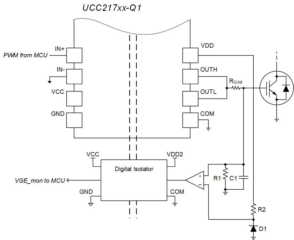
3.5.4 Power Switch Gate Voltage (VGE/VGS) Monitoring
Gate voltage monitoring, as shown in , Figure 3-9 is used to ensure that the gate voltage is reaching the VDD level when IN+ is pulled high. This is important to ensure the device is being driven efficiently to reduce switching loss and is held on at the proper voltage level to reduce conduction loss. The gate voltage is compared to VDD, with a small voltage divider to account for the gate voltage drop due to the gate resistance, RG,tot. The comparator's output is sent back to the MCU using a digital isolator. In case of a fault, the secondary bias supply should also be checked. This function may also be used to monitor VGE when DESAT or OC detection has been detected to ensure proper turn off when the gate is pulled low by the driver.
 Figure 3-9 VGE Monitoring Circuit