SLUAA69 July 2020 – MONTH TPS548D22
4.1 Negative OCP Functionality
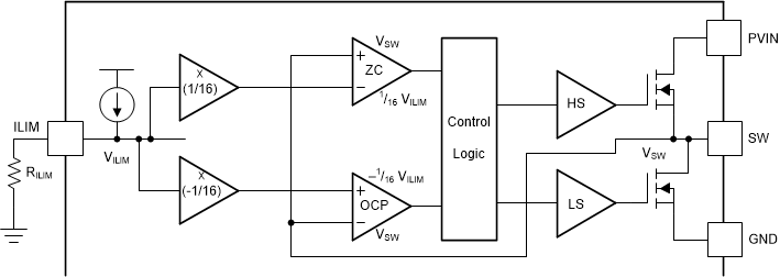
TPS548D22 has cycle-by-cycle overcurrent limit control. The inductor current is monitored by the voltage across low-side MOSFET RDS (on) during the OFF state. The controller maintains the OFF state during the period when the inductor current is larger than the overcurrent trip level. The device uses the GND pin as the positive current sensing node. As the comparison occurs during the OFF state, VILIM sets the valley level of the inductor current. Also, this device performs both positive and negative OCP with the same magnitudes. Positive current limit is normally used to protect the inductor from saturation which causes damage to MOSFETs. Negative current limit is normally used to protect the low-side MOSFET during OVP discharge. While in a synchronous buck converter with sinking current application, a negative current limit is also used to protect the inductor from saturation, just as the positive current limit does.
 Figure 4-1 OCP Functionality Block
Diagram of TPS548D22
Figure 4-1 OCP Functionality Block
Diagram of TPS548D22For positive OCP, once the magnitude of sensing voltage VSW (VSW is negative, since current follows from source to drain) exceeds -1/16 VILIM, the OCP comparator outputs high and a positive OCP event is recorded. For negative OCP, the detect threshold is set at the same absolute value as positive OCP but with negative polarity. Once the magnitude of sensing voltage VSW (VSW is positive, since current follows from drain to source) exceeds 1/16 VILIM, the ZC comparator outputs high and a negative OCP event is recorded. Note that the negative OCP threshold still represents the valley value of the inductor current.