SLUAAH0 February 2022 UCC14130-Q1 , UCC14131-Q1 , UCC14140-Q1 , UCC14141-Q1 , UCC14240-Q1 , UCC14241-Q1 , UCC14340-Q1 , UCC14341-Q1 , UCC15240-Q1 , UCC15241-Q1
- Trademarks
- 1 Introduction
- 2 Three-Phase Traction Inverter
- 3 Gate Drive Bias Requirements
- 4 Single Positive Isolated Output Voltage
- 5 Dual Positive and Negative Output Voltages
- 6 Dual Positive Output Voltages
- 7 Capacitor Selection
-
8 RLIM
Current Limit Resistor
- 8.1 RLIM Functional Description
- 8.2
RLIM
Dual Output Configuration
- 8.2.1 CVEE Above Nominal Value CVDD Below Nominal Value
- 8.2.2 CVEE Below Nominal Value CVDD Above Nominal Value
- 8.2.3 Gate Driver Quiescent Current: IQ_VEE > IQ_VDD
- 8.2.4 Gate Driver Quiescent Current: IQ_VEE < IQ_VDD
- 8.2.5 CVEE Above Nominal Value CVDD Below Nominal Value: IQ_VEE > IQ_VDD
- 8.2.6 CVEE Below Nominal Value CVDD Above Nominal Value: IQ_VEE < IQ_VDD
- 8.3 RLIM Single Output Configuration
- 9 UCC14240-Q1 Excel Design Calculator Tool
- 10Thermal Considerations
- 11Enable (ENA) and Power Good (/PG)
- 12PCB Layout Considerations
- 13Reference Design Example
- 14Summary
- 15References
11 Enable (ENA) and Power Good (/PG)
The UCC14240-Q1 includes a primary referenced, 5-V TTL and 3.3-V LVTTL logic compatible, active-high enable function. Forcing ENA low disables the device, and places it in a non-switching standby mode where current consumption is reduced to less than 500 µA. Pulling the ENA pin high, above the 2-V threshold, activates normal device functionality. The ENA pin has a weak internal pull-down resistor, so the ENA pin floats to the disable state if the pin is left open. If ENA is not used it should be pulled high a voltage between 2.5 V<VENA<5.5 V. Care should be taken to assure VENA does not exceed 5.5 VMAX.
The active-low, power good (/PG) pin is an open-drain output that indicates when the UCC14240-Q1 has no faults present and the output voltages are within ±10% of their regulation setpoints. Connect a pull-up resistor (>1 kΩ) from the /PG pin to either a 5-V or 3.3-V logic rail. For applications not using the /PG signal, /PG can be connected directly to GNDP.
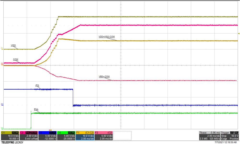
The start-up waveforms in Figure 11-1 show the expected behavior of /PG relative to ENA. The input voltage (VIN=24 V, not shown) is already present and the UCC14240-Q1 is activated by ENA going high. The measured time between ENA high and /PG low is ~3.75 ms but can vary according to the time required for the isolated output voltages to be within ±10% of the set regulation value. The longer time required for COM-VEE to reach regulation relative to VDD-VEE results in the slight VDD-COM overshoot but this is happening before /PG reaches its active-low state. This emphasizes the importance of not switching the gate driver until /PG is in the active-low state. Note that the waveforms introduced here, were captured from the UCC14240EVM-052 EVM. Using the UCC14240EVM-052 for Biasing Traction Inverter Gate Driver ICs Requiring Single, Positive or Dual, Positive/Negative Bias Power is the EVM User's Guide containing the schematic, PCB details and measured performance data.

Figure 11-1 Start-up: VIN=24 V, IDD=80 mA, (top: VISO (VDD-VEE), 10V/div, mid-1: COM, 2V/div, mid-2: VDD=VISO-COM, 10V/div, mid-3: VEE=-COM, 5V/div, mid-4: /PG, 5V/div, bot: ENA, 5V/div), time = 2ms/div unless otherwise noted.
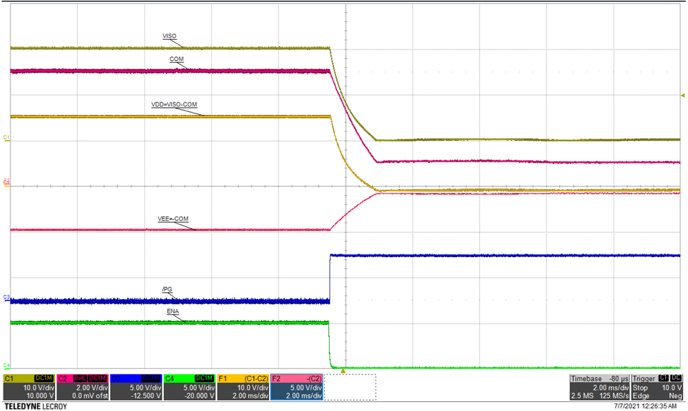
Conversely, the shut-down waveforms in Figure 11-2 show that as soon as ENA is pulled low, the UCC14240-Q1 output voltage are discharged in a controlled manner and /PG transitions high with almost no delay relative to ENA.

Figure 11-2 Shutdown: VIN=24 V, IVDD=80 mA, (top: VISO (VDD-VEE), 10V/div, mid-1: COM, 2V/div, mid-2: VDD=VISO-COM, 10V/div, mid-3: VEE=-COM, 5V/div, mid-4: /PG, 5V/div, bot: ENA, 5V/div), time = 2ms/div unless otherwise noted.