SLUAAM0 August 2022 LM5113 , LM5113-Q1 , LMG1020 , LMG1025-Q1 , LMG1205 , LMG1210 , UCC27611
GaN Parameter Advantages
GaN provides many advantages in relation to its parameters. GaN transistors’ Rds(on) value (drain to source on-state resistance) is very low in comparison to silicon which reduces conduction losses leading to more efficient devices.
GaNs total gate charge (total charge that accumulates at the gate terminal) is a lot lower, which results in faster switching and reduction in the gate drive losses.
Since a GaN FET has no body diode, a GaN FET also has zero reverse recovery charge, thus no reverse recovery losses.
GaN FETs have lower values compared to other transistors when it comes to the maximum allowable gate-to-source voltage (Vgs) and the threshold voltage.
Parasitics
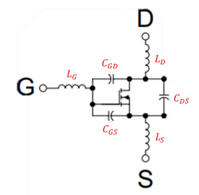
Similar to a MOSFET, GaN FETs also have parasitic capacitances between each terminal and parasitic inductances at each terminal. The input capacitance Ciss is the sum of Cgs and Cgd.
The output capacitance Coss is the sum of Cds and Cgd. The feedback capacitance or the reverse transfer capacitance Crss is simply Cgd.
 Figure 1-1 GaN FET Parasitic Model
GaN Parasitic Advantages
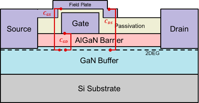
The lateral structure of the enhanced GaN FET also makes it a very low capacitance device. In this lateral structure, the gate-to-source capacitance is the capacitance of the device from the 2DEG channel (2 - dimensional electron gas) to the field plate on top of the gate terminal. It consists of the junction from the gate in channel, and the capacitance of the dielectric between the gate and the field plate.
The drain-to-source capacitance is the capacitance between the field plate and the drain terminal from the channel. The value of Cds is limited to the capacitance across the passivisation layer from the field plate to the drain.
Lastly, the gate-to-drain capacitance is located in a small portion of the gate terminal connected to the channel.
 Figure 1-2 GaN FET Basic Lateral Structure with Labeled Parasitic Capacitance
When it comes to the sizes of these capacitances, Cgd is smaller in size relative to the Cgs and Cds and Cds is smaller than Cgs. Since Cgs is larger than Cgd, the GaN FET has good dv/dt immunity and the capacitance’s size is still smaller relative to Si MOSFETs’.
With these smaller capacitances, the values for input and output capacitance, Ciss and Coss, are lower than Si FETs’ which is the key to faster switching and more efficiency.
Advantages of GaN FETs' Structure
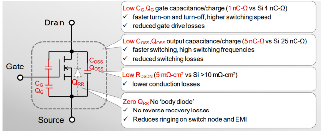
A GaN FET has a lateral structure which enables it to have a low gate capacitance, gate charge, output charge, and output capacitance. The advantages of GaN FETs' lateral structure enables higher switching speeds with reduced gate drive losses and reduced switching losses. GaN FETs also have a low RDS(ON) value which helps reduce conduction losses. Additionally, GaN FETs have zero reverse-recovery charges which leads to no reverse recovery losses and helps reduce ringing on the switch node as well as reduce electromagnetic interference.
 Figure 1-3 GaN FET Basic Lateral Structure Summarized Key Advantages
GaN FETs have a low threshold voltage which is due to its lateral structure, low CGD, and its relationship between threshold and temperature which is almost flat. The low threshold voltage means that there is low power dissipation that can result in more efficient switching. Once the gate threshold voltage is reached there will be enough electrons under the gate to form a conducive channel. This eliminates the minority carriers which are involved in conduction and aids in no reverse recovery losses.
Operating Conditions
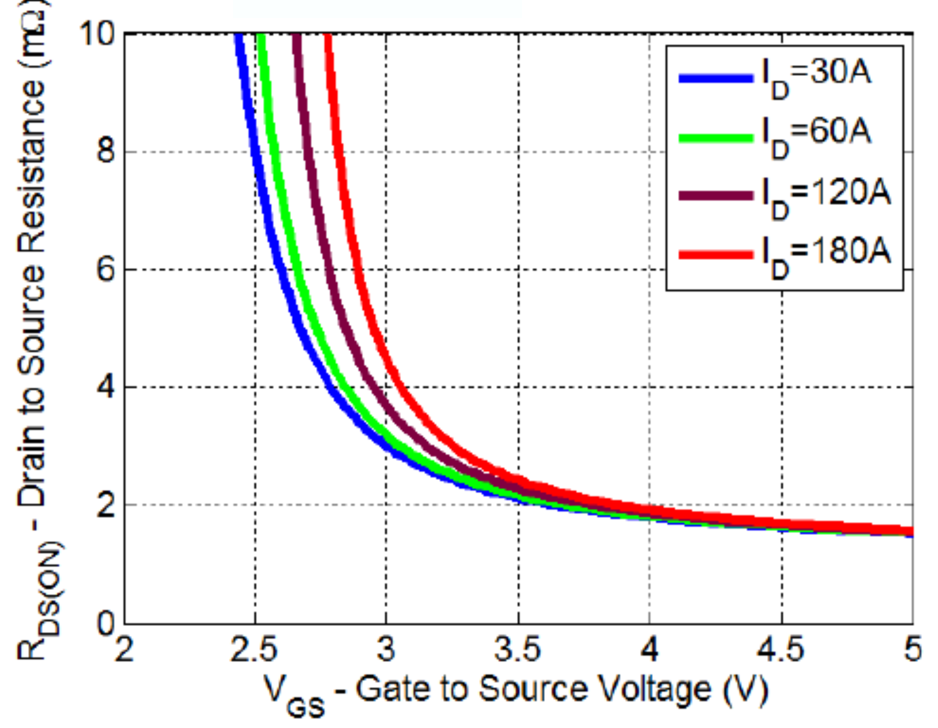
GaN can be sensitive, so deviating from the recommend operating conditions might cause issues. Firstly, GaN has a limited gate voltage range. A typical recommended operating turn-on gate voltage is 5 V with 6 V generally being the maximum value. The recommended gate voltage for turn-off is -2 V to avoid any non-desired turn-on events that could occur due to high voltage changes. These values can be different depending on the application or parts, therefore it is best to refer to the data sheets of the devices to enable the best performance. Examples of two GaN drivers that can help regulate the voltage to drive the FET at the appropriate voltage utilizing an internal LDO (low dropout) are the LMG1210 and UCC27611.
To take advantage of the GaN technology benefits it is important to use a GaN specific driver in combination with a GaN FET, as GaN drivers have certain characteristics that make them better suited to drive GaN FETs. These characteristics include having high peak output currents which help with the turn on and turn off efficiencies. Additionally, the speed of the switching characteristics is also important to achieve the fastest speeds possible using the driver and FETs.
 Figure 1-4 Optimal GaN Drive Voltage
TI GaN Driver Portfolio
In TI’s GaN gate driver portfolio, there are currently 6-product, 3 half-bridge gate drivers (LMG1205, LMG1210, LM5113-Q1) and 3 low-side gate drivers (LMG1020, LMG1025, UCC27611). For both the half bridge and low side grate drivers, there is one automotive qualified part. Our drivers have low propagation delays with individual features that make each driver different. Some notable features include: controllable dead time, bootstrap supply voltage clamps, internal bootstrap diodes, and an internal LDO for our half-bridge drivers. Similarly, our low-side drivers can feature an internal LDO and nanosecond pulse width capabilities. A certain driver might be more suited for an application than another, so it is always best to check which driver best fits your requirements.