SLUP412 February 2022 LMG3522R030-Q1
- 1 Introduction
- 2 Comparing Different Technologies
- 3 Advantages of Integrating the Driver With GaN FETs
- 4 The GaN-Based 6.6-kW OBC Reference Design
- 5 PFC Stage
- 6 DC/DC Stage
- 7 DC/DC Topology Selection
- 8 Frequency Selection
- 9 Core Loss
- 10Loss of ZVS
- 11Dead Time
- 12ISR Bandwidth
- 13Overall
- 14Resonant Tank Design
- 15Thermal Solution
- 16Layout Best Practices
- 17Control-Loop Considerations
- 18Conclusions
- 19References
- 20Important Notice
17 Control-Loop Considerations
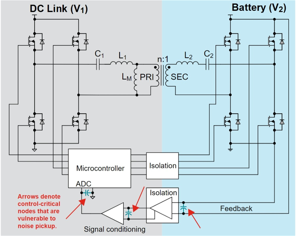
Figure 17-1 shows the control system block diagram for the DC/DC converter. Because the system is isolated, it is necessary to cross the isolation barrier twice: once to deliver the control signals to the secondary-side GaN FETs and once to provide feedback to the MCU residing on the primary side.
The purpose of the feedback control loop is to minimize the impact of the PFC 100-/120-Hz output voltage ripple on the CLLLC output current, maintain stability and prevent jitter. Essentially, the control loop needs to manage the bandwidth to charge the battery while preventing excessive currents in that battery. In general, it is possible to achieve low ripple battery currents with 1 to 2 kHz of bandwidth.
Given that GaN enables a higher switching frequency, the bandwidth is mostly limited by the need to prevent unwanted jitter. One of the biggest limiters to bandwidth is noise pickup on the board. Since the noise travels a long distance through many stages across the secondary, it’s critical to filter this path. The long noise-sensitive routing is compounded by the fact that both the PFC and CLLLC are using one MCU, thus necessitating both good layout and proper filtering.
Noise-free feedback is essential to jitter-free operation. Proper layout is always the best line of defense; however, practical layout constraints always results in the pickup of noise. Once that noise is on the feedback node, the large gains in the compensator can produce significant pulse-width jitter. Fortunately, adding capacitance can suppress this noise.
One good place to add capacitance is at the output of the voltage divider. The high-voltage output requires the use of large resistor values to create the divider. In addition to filtering noise, the capacitance at the feedback point creates a pole with those resistors. Preventing this pole from interfering with the required bandwidth necessitates a relatively small capacitor. The constraints on current feedback are not the same as voltage feedback.
This design uses a low-ohmic resistor for sensing, which enables the use of larger capacitors on the current feedback lines. Using a high-quality high-quality operational amplifier (op amp) to properly condition the signal will enable more heavy filtering of the analog-to-digital converter (ADC) input when placed directly on the ADC pin inputs. The ability to put capacitance on the ADC input pins is dependent on the op amp's ability to drive a capacitive load, which should be listed in the data sheet. It is best to place some capacitance in each location (Figure 16-5); however, with proper op-amp selection selection, the ADC pins may be the most effective location to filter.
In addition to capacitance, the MCU also uses oversampling and averaging of the ADC measurements to further reduce noise and increase the effective number of bits.
 Figure 17-1 Control-loop block
diagram.
Figure 17-1 Control-loop block
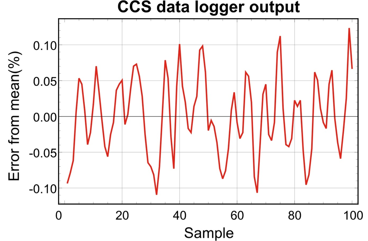
diagram.Figure 17-2 shows what the MCU ADC output looks like after adding proper filtering to the system. Notice that the error floor is roughly within ±0.1%, a percentage that was definitely sufficient for the design, but on the surface might also seem small.
 Figure 17-2 ADC feedback noise
floor.
Figure 17-2 ADC feedback noise
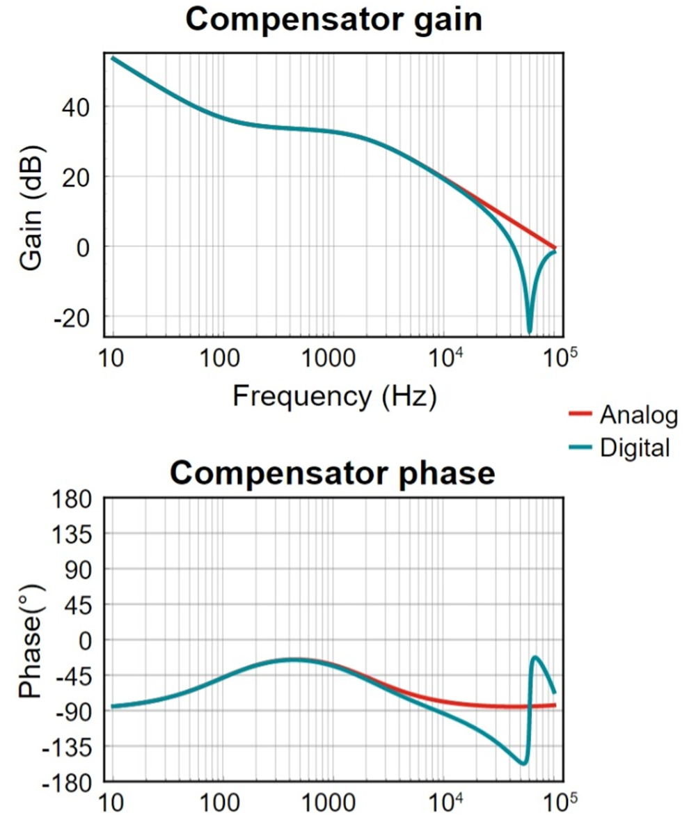
floor.Figure 17-3 shows the gain and phase of the compensator as designed to deliver the required performance. When controlling a large output voltage (400 V) a large attenuation is required to get the signal to a level that the MCU can sense (typically less than 3.3 V). In order to get a reasonable bandwidth out of the system, the compensator may require a gain of 30 dB or more. A gain that large can make the system sensitive to very small noise variations.
 Figure 17-3 Compensator Bode plot.
Figure 17-4 shows the final Bode plots across load for both voltage and current feedback operation, with the former operating into a constant current load and the latter operating into a constant voltage load. What you cannot see with these plots is that in all cases, the duty-cycle modulation is well controlled without excessive jitter.