SLUU286A March 2008 – October 2021 TPS54286 , TPS54386
- Trademarks
- 1Introduction
- 2TPS54386EVM Electrical Performance Specifications
-
3Schematic
- 3.1 Sequencing Jump (JP3)
- 3.2 Enable Jumpers (JP1 and JP2)
- 3.3
Test Point Descriptions
- 3.3.1 Input Voltage Monitoring (TP1 and TP2)
- 3.3.2 Channel 1 Output Voltage Monitoring (TP3 and TP4)
- 3.3.3 Channel 1 Loop Analysis (TP5, TP6, TP7 and TP8)
- 3.3.4 Channel 1 Switching Waveforms (TP9 and TP10)
- 3.3.5 TPS54386 Device Ground (TP11)
- 3.3.6 Channel 2 Switching Waveforms (TP12 and TP13)
- 3.3.7 Channel 2 Loop Analysis (TP14, TP15, TP16 and TP17)
- 3.3.8 Output Voltage Monitoring (TP18 and TP19)
- 44 Test Set Up
- 5TPS54386EVM Typical Performance Data and Characteristic Curves
- 6EVM Assembly Drawings and Layout
- 7List of Materials
- 8Revision History
6 EVM Assembly Drawings and Layout
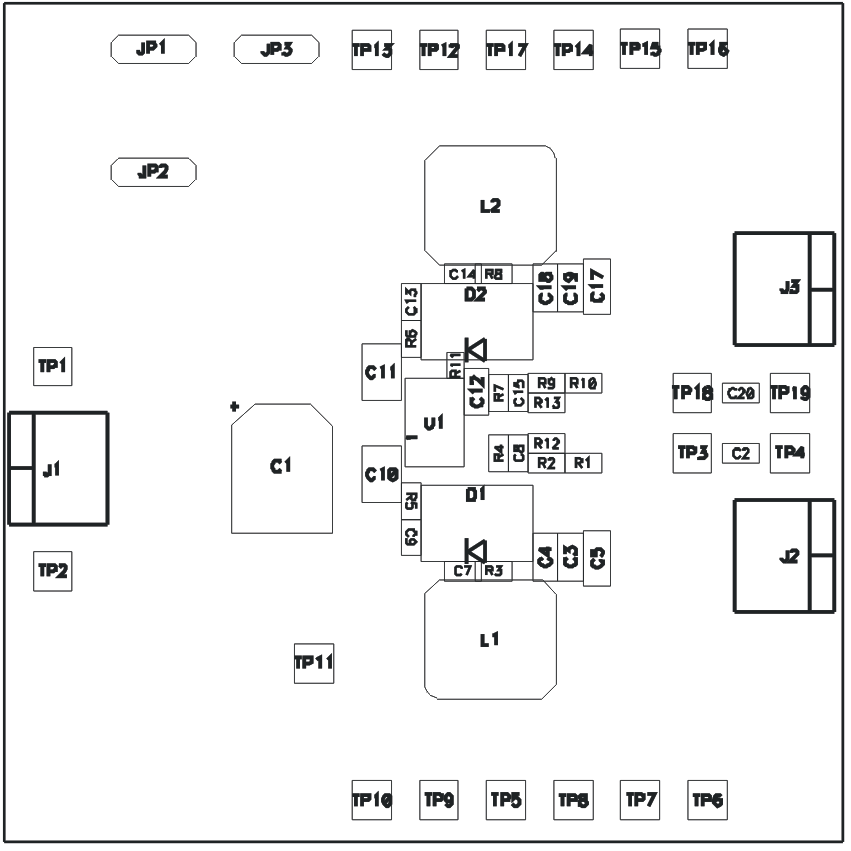
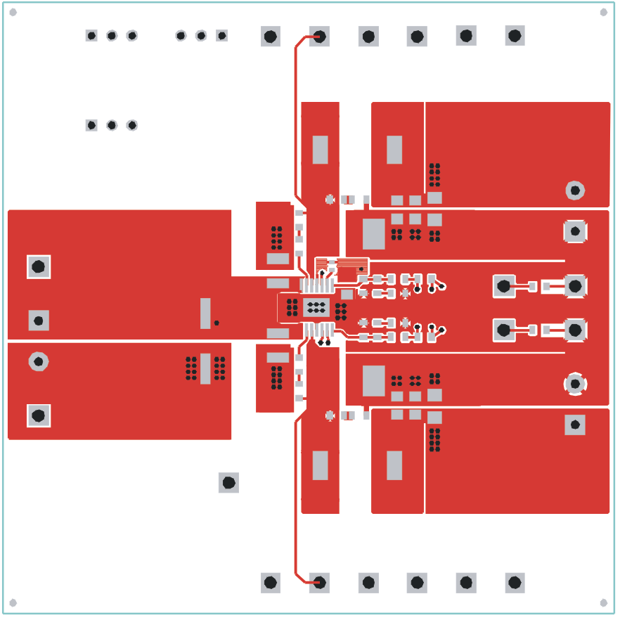
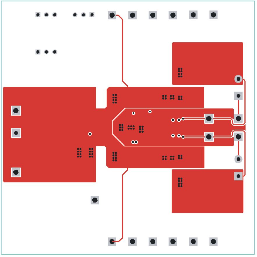
The following figures (Figure 6-1 through Figure 6-3) show the design of the TPS54386EVM printed circuit board. The EVM has been designed using a 4-Layer, 2-oz copper-clad circuit board 3.0” x 3.0” with all components in a 1.15” x 2.15” active area on the top side and all active traces to the top and bottom layers to allow the user to easily view, probe and evaluate the TPS54386 control device in a practical double-sided application. Moving components to both sides of the PCB or using additional internal layers can offer additional size reduction for space constrained systems.
 Figure 6-1 TPS54386EVM Component Placement (viewed from top)
 Figure 6-2 TPS54386EVM Top Copper (viewed from top)
 Figure 6-3 TPS54386EVM Bottom Copper (x-ray view from top)