SLVAE30E February 2021 – March 2021 TPS1H000-Q1 , TPS1H100-Q1 , TPS1H200A-Q1 , TPS1HA08-Q1 , TPS25200-Q1 , TPS27S100 , TPS2H000-Q1 , TPS2H160-Q1 , TPS2HB16-Q1 , TPS2HB35-Q1 , TPS2HB50-Q1 , TPS4H000-Q1 , TPS4H160-Q1
- Trademarks
- 1Introduction
- 2Driving Resistive Loads
- 3Driving Capacitive Loads
- 4Driving Inductive Loads
- 5Driving LED Loads
- 6Appendix
- 7References
- 8Revision History
2.4.2 PWM and Switching Loss
Calculating just the power dissipation and junction temperature at steady state operation is the first step to choosing a smart high side switch to drive resistive loads. As mentioned in the application section, most resistive loads work by PWMing the switch to adjust the amount of current given to the load. This PWMing, or the turning on and off rapidly of the switch, introduces more loss in the switch that also needs to be accounted for in large load current applications. Most designers' assumption at this point would be that since the load is resistive there wouldn't be any power losses when turning it on and off because from Ohm's law the voltage is directly proportional to the current. Therefore, when the current goes to zero the voltage will follow. There are two problems with this assumption. The first is that there is no such thing as a purely resistive load as real world parasitics in the load must be accounted for and will directly affect the relationship of the voltage and current. The second, and more prominent, is that the smart high side switches are designed to have a set shape for the output voltage waveform. This means that when the system is PWMing the enable pin of the switch, the output voltage waveform will not directly mirror enable. It will instead have a different slew rate by design. It is very important and necessary that the switch does this because very quick changes in the output waveform will emit large amounts of EMI that can be disruptive especially in automotive systems. The shape of the turn on and turn off pulse is defined in the datasheet. Figure 2-4 shows an example waveform.
 Figure 2-4 Smart High Side Switching Waveform
The smart high side switch's datasheet defines the turn on delay, td(on) or tDR, and the total turn on time, td(rise) or tON, and the subtraction of the two gives the 10% to 90% rise time for the output device. In the same way, the turn off delay, td(off) or tDF, and the total turn off time, td(fall) or tOFF, can be used to find the 90% to 10% fall time for the output. This does not, however, tell the entire story as there are extra switching losses that happen from 0-10% and 10-0%. Using Figure 2-5 it can be seen that the switching energy loss is the area under the power dissipation curve for the turn on and turn off times.
 Figure 2-5 Switching Energy Losses during PWM
This image shows the voltage across the main FET, VDS, of the switch and the current through the system, IOUT. Underneath these waveform shows the power dissipation waveform which is the multiplication of the two waveforms above. Clearly the VDS and IOUT are inversely proportional. Their waveform is not linear which can be seen by the spikes on the power waveform in red for the turn on and turn off periods. Until the system gets to the steady state, the area under this curve is what is referred to as the switching on or off energies, EON and EOFF. It is important to note that this is a visual representation and is not drawn to exact scale as the main energy loss will be the dissipation through the FET in most cases.
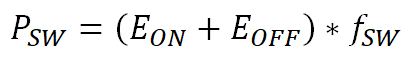
The lower the RON of the switch the more prevalent the switching losses become. Therefore, TI has provided the switching energy losses during turn off and turn on for the low RON family of devices. Taking this value, in mJ, and multiplying it by the switching frequency will give the switching energy losses.
It is also important to note that this is the switching loss for one channel. If the device has more than one channel the switching loss plus the FET dissipation is multiplied by the number of channels

Now that when the power loss due to switching has been determined the total power dissipation in the system can be calculated to confirm that the device can drive this load successfully. This is as simple as adding up all of the switching losses and power dissipation losses for the total power dissipation and using Equation 5 to calculate the junction temperature. If the junction temperature is below the thermal shutdown threshold then the device can successfully deliver power to the load.
| Smart Power Switch | TPS2HB16-Q1 |
|---|---|
| Resistive Load 1 , RH1 | 1.42 Ω |
| Resistive Load 2, RH2 | 2.6 Ω |
| Battery Voltage, VBAT | 13.5 V |
| PWM Frequency 1, fSW1 / Duty Cycle, D1 | 200Hz, 50% |
| PWM Frequency 2, fSW2 / Duty Cycle, D2 | 100Hz, 85% |
| Ambient Temperature, TA | 70°C |
| RθJA, JEDEC | 32.9 W/°C |
| TABS | 160°C |
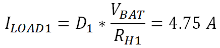
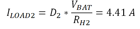
An example would be if we have two resistive heater loads: the first one is 1.42Ω and needs to be switched at 200Hz with a 50% duty cycle and the second one is 2.6Ω and is PWMed at 100Hz with a 85% duty cycle. The battery voltage is 13.5V. Using TPS2HB16-Q1 and knowledge of resistive loads we can first calculate the steady state load current for both IH1 for channel 1 and IH2 for channel 2.
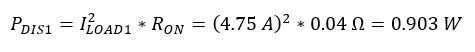
The next step is to calculate the power dissipation of the switch during normal operation for each channel using Equation 4. Note also that the RON value comes from "On Resistance (RON) vs Temperature" graph in the TPS2HB16-Q1 datasheet. The natural question that arises is if the load with the duty cycle factored in acceptable to use in power dissipation calculations. This is a question because in Figure 2-5 there is no concern about the duty cycle for the PDIS potion of the energy loss. This is mitigated by the fact that this is a steady state calculation. This means that as long as the duty cycle does not change dynamically the average power dissipation through the switch will be related to the steady state current calculated with the duty cycle.

Now that the nominal power dissipation of the switch has been calculated the switching losses must be added. In the TPS2HB16-Q1 datasheet the EON is defined as 0.4mJ and the EOFF is also defined as 0.4mJ. Using Equation 6 the switching loss for the device can be found.


This can be seen in the waveforms below. Figure 2-6 shows the switching of the RH1 with the blue waveform being the enable signal, the green being the VBB, the yellow is the VOUT and the purple is the IOUT. Also, in Figure 2-7, the VDS of the switch can be seen in white and the resulting power dissipation with the switching losses is in red.
 Figure 2-6 Measured Switching Waveform
 Figure 2-7 Measured Switching Losses Waveform
Adding up all of the losses in the device gives the total power dissipation.

Finally, now that the total power dissipation has been determined, the junction temperature can be calculated using Equation 5.
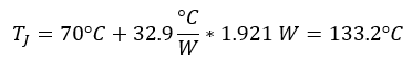
This temperature is much lower than the 160°C thermal shutdown of the device meaning the TPS2HB16-Q1 can safely drive these loads.