SLVAEW7 September 2020 ADC12DJ5200RF , LMK00304 , LMK04828 , LMX2594 , TPS62912 , TPS62913
2.1 Test Methodology
Power Supply Rejection Ratio (PSRR)
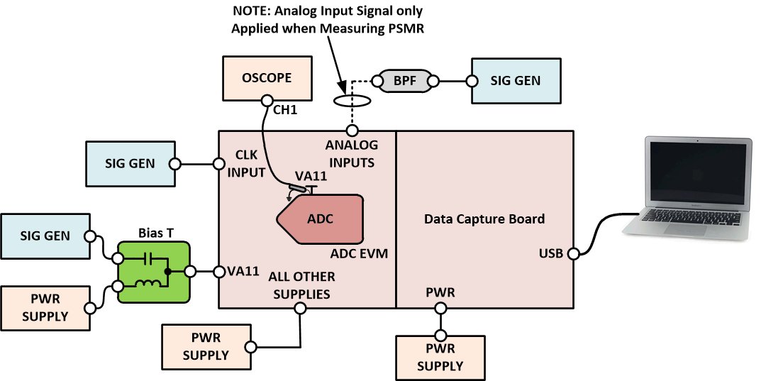
The PSRR is typically measured as shown in Figure 2-1using HSDC-Pro software to display and measure the digital output FFT spectrum. Each supply is tested individually, using a bias T, which can be purchased off the shelf from various companies. The bias T is used to combine the AC and DC signal to the individual supply under test. It’s worth noting that the bias T must have a high enough current rating to supply enough bias to the supply under test. If not, the measurement could produce unreliable results.
After setting up the EVM or system board as you normally would, next, isolate the supply under test. Then apply the bias T to that supply, setting the appropriate DC voltage using an external lab bench power supply. Apply power to the rest of the board’s power supplies as you normally would, keeping those supplies at nominal. Next, select a low frequency, 10 MHz or less to start and inject the sinewave signal source to the bias T. This is called the error signal. It is also important to use a signal generator that is used for the applied error signal, is clean with low phase noise. This is so that the converter’s inherent performance is not otherwise degraded during testing. The signal generator should also be able to provide enough power to accommodate for the losses through the cabling, bias T and pcb.
Start the signal low in amplitude, slowly bringing the amplitude up until a spur comes out of the noise floor, the error spur should be high enough in the FFT spectrum where it is repeatable. The error spur should show at the error test frequency injected. Lets say the error spur amplitude captured is -85 dB.
Next use an oscilloscope or spectrum analyzer to note the level of the error signal injected. Make sure the error signal amplitude reading is taken at the ADC’s power pin and note the peak to peak voltage injected at that pin. Once this is found, PSRR can be found using some simple math.
For example, if the voltage measured was 10mVpp and the converter’s fullscale voltage is 1.2 Vpp. Then simply take the ratio of those two numbers or 20*log(10m/1.2) = -41.6 dB. To find PSRR, subtract this number from the error spur amplitude found previously in the FFT spectrum or PSRR = -85 - -41.6 = -43.4 dB.
 Figure 2-1 Test Configuration for PSRR
and PSMR Measurement
Figure 2-1 Test Configuration for PSRR
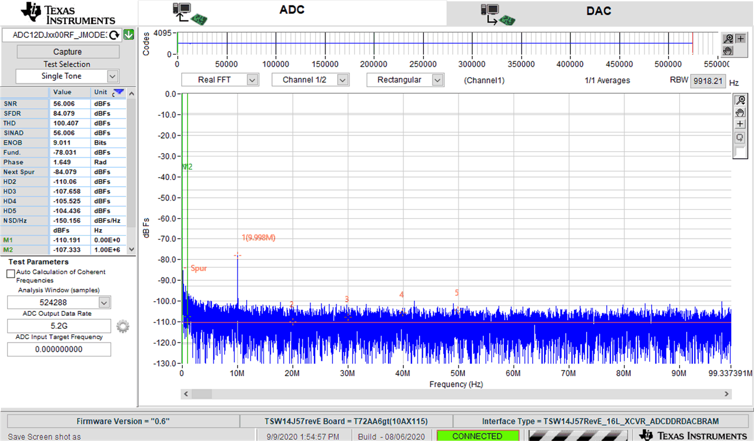
and PSMR MeasurementAn example of PSRR, with a forced error signal injected on the VA11 supply at 10 MHz with a -1 dBm amplitude level from the signal generator is shown in Figure 2-2.
 Figure 2-2 Example of Power Supply Rejection Ratio with Forced Error Signal
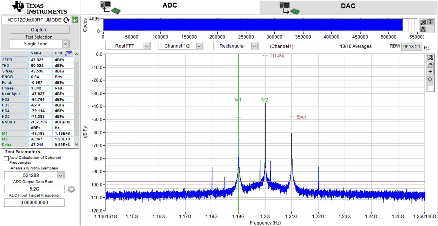
An example of PSMR, with a forced error signal injected at 10 MHz with a -1 dBm amplitude level from the signal generator is shown in Figure 2-3. This figure proves how leaky spurs through a power supply can modulate, 10 MHz in this example, with the analog input signal frequency of 1.2 GHz. Notice the 10 MHz sidebands off the carrier signal and its intermodulation spurs within the same area.
 Figure 2-3 Example of Power Supply Modulation Ratio with
Forced Error Signal
Figure 2-3 Example of Power Supply Modulation Ratio with
Forced Error SignalSignal-to-Noise Ratio (SNR, dBFS)
The SNR is the ratio of the rms signal amplitude to the rms value of the sum of all spectral components excluding DC, HD2 to HD9, fS / 2, fS / 2 – fIN. The difference between SNR (dBc) and SNRFS is the difference between the fundamental amplitude and full scale.
Harmonic Distortion (dBc or dBFS)
A harmonic is a spectral component that is an integer multiple of the driven analog input frequency. For example, the frequency of the second harmonic is twice the analog input. Most ADCs have specifications for one or more harmonics. Typically, the second and third harmonics are singled out because they account for the worst performance of all the harmonics. Harmonic distortion, no matter the order, is the ratio of the rms signal amplitude to the rms value of the specified harmonic component, reported in dBc or dBFS. ADCs are nonlinear devices, therefore output FFT captured will be rich in spectral components.
Spurious-Free Dynamic Range (SFDR, dBc or dBFS)
The SFDR is the ratio of the rms value of the signal to the rms value of the peak spurious spectral component for the analog input frequency that produces the worst result. In most cases, SFDR is either the second or third harmonic (HD2 or HD3) of the input signal applied to the ADC.
Noise Spectral Density (NSD, dBFS/Hz)
The NSD is defined the entire noise power, per unit of bandwidth, sampled at an ADC’s input. NSD is effectively the ADCs’ SNR plus the power of the noise spread across the entire Nyquist band, which is equal to half the sample frequency, or Fs/2. Therefore, NSD = SNR + 10*log(Fs/2).
 Figure 2-4 Test Configuration for SNR, SFDR, HD, and NSD
Measurement
Figure 2-4 Test Configuration for SNR, SFDR, HD, and NSD
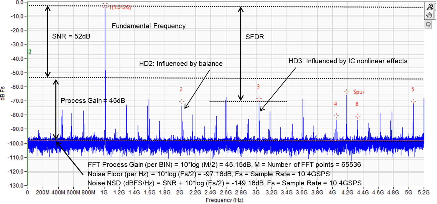
MeasurementFor a visual description of how to read SNR, SFDR, Harmonic Distortion, and NSD, refer to Figure 2-5.
 Figure 2-5 FFT showing SNR, SFDR, NSD, and
Harmonic Distortion