SLVAF10 March   2021 TPS1H000-Q1 , TPS1H100-Q1 , TPS1H200A-Q1 , TPS1HA08-Q1 , TPS1HB08-Q1 , TPS1HB16-Q1 , TPS1HB35-Q1 , TPS1HB50-Q1 , TPS2H000-Q1 , TPS2H160-Q1 , TPS2HB16-Q1 , TPS2HB35-Q1 , TPS2HB50-Q1 , TPS4H000-Q1 , TPS4H160-Q1


  1.   Trademarks
  2. 1Introduction
  3. 2Device Thermals
  4. 3Timing Limitations
    1. 3.1 Background
    2. 3.2 Pulse-Width distortion (PWD)
      1. 3.2.1 Timing Impact of Delay Mismatch
      2. 3.2.2 Power Impact of Delay Mismatch on Resistive Loads
    3. 3.3 Finite Slew Rate
      1. 3.3.1 Timing Impact of Finite Slew Rate and Slew Rate Mismatch
      2. 3.3.2 Impact of Finite Slew Rate on Resistive Load Power
      3. 3.3.3 Impact of Slew Rate on LED Power
  5. 4System-Level Considerations
    1. 4.1 Diagnostics and Protection
      1. 4.1.1 Analog Current Sense
    2. 4.2 Dimming Ratio
    3. 4.3 Side-Stepping Frequency Limitations
  6. 5References

Device Thermals

Thermal limits of any IC should always be kept in mind, and this is especially true for high-side switches which are often asked to switch large currents to the load.

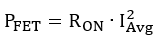
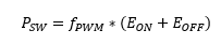
We can estimate the total power dissipated by the device itself by summing power dissipation due to the FET RON, switching losses, and quiescent power.

We can calculate power dissipated in the HSS FET as in Equation 1. This power is proportional to the on-resistance (specified in the device datasheet) and the average current through the FET.

Equation 1. GUID-8BF48B40-9A97-4E47-BE7E-467DFAE6B474-low.png
As PWM operation switches the HSS FET on and off every cycle, we also need to consider how much energy it takes to charge and discharge the gate. We can use Equation 2 to calculate switching loss from switching energy losses EON, EOFF if defined in the device datasheet. Notably, this scales with frequency and is a large component of total power dissipation in the HSS.

Equation 1. GUID-20210301-CA0I-TBWX-SSRC-NGQBMFQKXHNL-low.png
If EON, EOFF are not available for a device, we can approximate the switching losses from how long it takes the device to slew the output low or high using Equation 3.

Equation 1. GUID-AE36703F-F3C7-4708-B3D6-694ACAD62C73-low.png
We then substitute our results from Equation 3 into Equation 2 to get switching power.
Equation 1. GUID-9133F194-8295-485C-A1D9-1F97209D222E-low.png
Equation 1. GUID-4EB56D77-2592-403A-B027-7B44A53A6D58-low.png
A safe junction temperature must be maintained whether operating in PWM or DC driving. The maximum limit is specified in the HSS datasheet—generally 150°C. TI HSS datasheets contain the thermal characterization parameters listed in Table 2-1

Table 2-1 Definitions of Thermal Parameters
RΘJAJunction-to-ambient thermal resistance
RΘJBJunction-to-board thermal resistance
RΘJCJunction-to-case thermal resistance.

TI HSSs utilize a thermal pad which is recommended to be soldered directly to the PCB. This benefits devices thermals by utilizing the large surface area of the attached thermal plane as a heatsink, which closely couples with board temperature. Board temperature, however, is difficult to measure accurately and is highly dependent on board construction and solder coverage/quality on the high side switch. Ambient temperature, on the other hand, is easier to measure and straightforward to use in junction temperature estimation.

For a given ambient temperature the operating junction temperature may be estimated as below.

Equation 1. GUID-25C2D901-656A-4068-B855-0BE8F553DD0E-low.png
The PWM frequency is set tightly by the maximum sustainable power dissipation of the HSS, as switching losses are dominant. This power limit can be estimated from Absolute max junction temperature specification and maximum ambient temperature.

Equation 1. GUID-92B2B7FE-5B39-4640-A98C-3591E9EE1648-low.png
GUID-BEC81091-DA9B-4947-B943-0C62C987946D-low.png
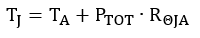
Figure 2-1 Power Dissipation Sources in TPS1HA08