SLVAF10 March 2021 TPS1H000-Q1 , TPS1H100-Q1 , TPS1H200A-Q1 , TPS1HA08-Q1 , TPS1HB08-Q1 , TPS1HB16-Q1 , TPS1HB35-Q1 , TPS1HB50-Q1 , TPS2H000-Q1 , TPS2H160-Q1 , TPS2HB16-Q1 , TPS2HB35-Q1 , TPS2HB50-Q1 , TPS4H000-Q1 , TPS4H160-Q1
3.2.1 Timing Impact of Delay Mismatch
If td(match) > 0, this means that the ON delay is larger than OFF delay. This results in truncation of a high PWM pulse by td(match). Conversely td(match) < 0 results in expansion of the high PWM pulse and truncation of the low pulse by td(match). Increased delay mismatch mutates the output PWM, which is why delay mismatch is also referred to as pulse-width distortion.
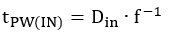
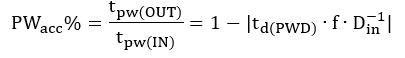
The actual pulse-width observed on the output can be calculated as below, where Din is the input PWM duty cycle and f is the PWM frequency. Using min/max data sheet specifications in these calculations gives the worst case pulse-widths versus frequency as well as the range guaranteed by TI.
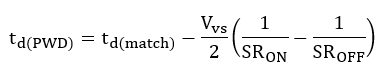
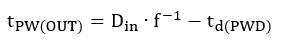
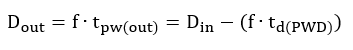
Figure 3-4, Figure 3-5 show the possible variation from ideal pulse width based on data sheet specifications for TPS1H100-Q1. Most devices will be well-matched and fall close to the ideal pulse-width curve, but as pulse-width decreases the output pulse-width may vary significantly for some devices.
 Figure 3-4 Device-to-Device Output
Pulse-Width Variation, D = 50%
Figure 3-4 Device-to-Device Output
Pulse-Width Variation, D = 50% Figure 3-5 Device-to-Device Output
Pulse-Width Variation, D = 10%
Figure 3-5 Device-to-Device Output
Pulse-Width Variation, D = 10%We can then take the pulse width accuracy compared to the input and correlate this into the formula below: