SLVS876D November 2008 – November 2014
PRODUCTION DATA.
- 1 Features
- 2 Applications
- 3 Description
- 4 Simplified Schematic
- 5 Revision History
- 6 Pin Configuration and Functions
- 7 Specifications
-
8 Detailed Description
- 8.1 Overview
- 8.2 Functional Block Diagram
- 8.3
Feature Description
- 8.3.1 Fixed-Frequency PWM Control
- 8.3.2 Voltage Reference (Vref)
- 8.3.3 Bootstrap Voltage (BOOT)
- 8.3.4 Enable and Adjustable Input Undervoltage Lockout (VIN UVLO)
- 8.3.5 Programmable Slow-Start Using SS Pin
- 8.3.6 Error Amplifier
- 8.3.7 Slope Compensation
- 8.3.8 Current Mode Compensation Design
- 8.3.9 Overcurrent Protection and Frequency Shift
- 8.3.10 Overvoltage Transient Protection
- 8.3.11 Thermal Shutdown
- 8.4 Device Functional Modes
-
9 Application and Implementation
- 9.1 Application Information
- 9.2
Typical Application
- 9.2.1 Design Requirements
- 9.2.2 Detailed Design Procedure
- 9.2.3 Application Curves
- 10Power Supply Recommendations
- 11Layout
- 12Device And Documentation Support
- 13Mechanical, Packaging, And Orderable Information
11 Layout
11.1 Layout Guidelines
The VIN pin should be bypassed to ground with a low ESR ceramic bypass capacitor. Care should be taken to minimize the loop area formed by the bypass capacitor connections, the VIN pin, and the anode of the catch diode. The typical recommended bypass capacitance is 10-μF ceramic with a X5R or X7R dielectric and the optimum placement is closest to the VIN pins and the source of the anode of the catch diode. The GND D pin should be tied to the PCB ground plane at the pin of the IC. The source of the low-side MOSFET should be connected directly to the top side PCB ground area used to tie together the ground sides of the input and output capacitors as well as the anode of the catch diode. The PH pin should be routed to the cathode of the catch diode and to the output inductor. Since the PH connection is the switching node, the catch diode and output inductor should be located very close to the PH pins, and the area of the PCB conductor minimized to prevent excessive capacitive coupling. For operation at full rated load, the top side ground area must provide adequate heat dissipating area. The TPS54232 uses a fused lead frame so that the GND pin acts as a conductive path for heat dissipation from the die. Many applications have larger areas of internal or back side ground plane available, and the top side ground area can be connected to these areas using multiple vias under or adjacent to the device to help dissipate heat. The additional external components can be placed approximately as shown. It may be possible to obtain acceptable performance with alternate layout schemes, however this layout has been shown to produce good results and is intended as a guideline.
11.2 Layout Example
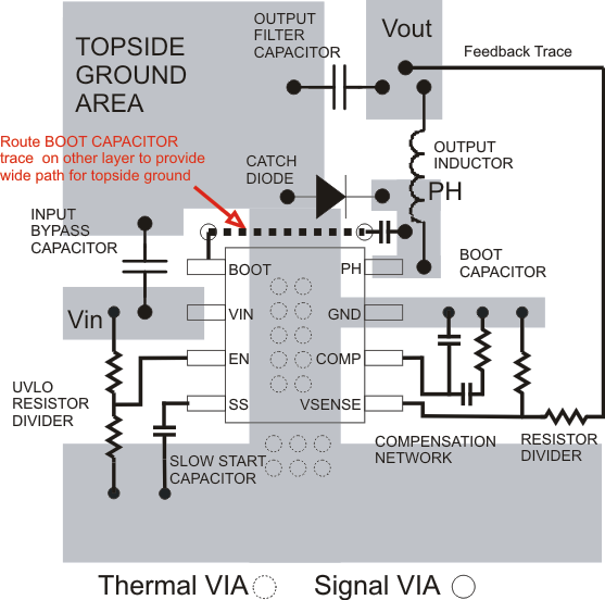 Figure 23. TPS54232 Board Layout
11.3 Estimated Circuit Area
The estimated printed circuit board area for the components used in the design of Figure 10 is 0.44 in2. This area does not include test points or connectors.
11.4 Electromagnetic Interference (EMI) Considerations
As EMI becomes a rising concern in more and more applications, the internal design of the TPS54232 takes measures to reduce the EMI. The high-side MOSFET gate drive is designed to reduce the PH pin voltage ringing. The internal IC rails are isolated to decrease the noise sensitivity. A package bond wire scheme is used to lower the parasitics effects.
To achieve the best EMI performance, external component selection and board layout are equally important. Follow the above to prevent potential EMI issues.