SLVUB50C June 2017 – March 2019 UCD90120A , UCD90124A , UCD90160 , UCD90160A , UCD90240 , UCD90320 , UCD90320U , UCD9090 , UCD9090-Q1 , UCD9090A , UCD90910
2.1 UCD90240, UCD90320 and UCD90320U
The UCD90240, UCD90320 and UCD90320U devices have the following power supply parameters:
- Pin A2, G13, M12, and N10 leave floating or isolated
- Pin G12, K11, M10 and N13 ties to DVSS
- K12 ties to V33D
- Three 1-μF X7R ceramic capacitors in parallel with two 0.1-μF X7R ceramic capacitors for BPCAP decoupling
- Two 1-μF X7R ceramic capacitors in parallel with four 0.1-μF X7R ceramic capacitors and two 0.01-μF X7R ceramic capacitors for V33D decoupling
- One 1-μF X7R ceramic capacitor in parallel with one 0.1-μF X7R ceramic capacitor and one 0.01-μF X7R ceramic capacitor for V33A decoupling. A 1-Ω resistor can be placed between V33D and V33A to decouple the noise on V33D from V33A.
- One 1-μF X7R ceramic capacitor in parallel with one 0.01-μF X7R ceramic capacitor for VREFA+ decoupling (if used)
- Place decoupling capacitors as close to the device as possible
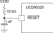
- If an application does not use the RESET signal, the RESET pin must be tied to V33D, either by direct connection to the nearest V33D pin, or by an R-C circuit as shown in Figure 1.
 Figure 1. RESET With R-C Network
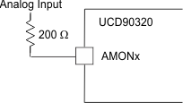
  Figure 2. Example of Analog Inputs