SLVUBI2A July 2018 – October 2020 TPS650330-Q1 , TPS650331-Q1
- Trademarks
- 1 Introduction
- 2 Requirements
- 3 Operation Instructions
- 4 EVM Configurations
- 5 Test Points
- 6 Graphical User Interface
- 7 Typical Performance Plots
- 8 TPS650330-Q1 EVM Schematic
- 9 TPS650330-Q1 EVM PCB Layers
- 10TPS650330-Q1 EVM Bill of Materials
- 11TPS650330-Q1 Silicon Revision Changes
- 12Revision History
6.2.4.1 Using Device Configuration to Define Spin Settings
In some circumstances, TI may provide customized, pre-programmed devices for the camera application. Contact a local TI sales representative for more information.
The Device Configuration tabs in the GUI can be used to define custom settings for TI to pre-program into the device Non-Volatile Memory (NVM). Before beginning the spin definition, see the Camera PMIC Spin Selection Guide to determine if there is an exisiting spin that is already compatible with the target application and the image sensor or both.
Since the visual instruments in the Device Configuration page link directly to the corresponding bits and registers in the Register Map page, the Device Configuration page can be used to quickly define desired OTP register settings.
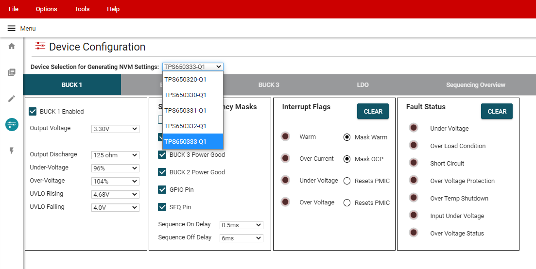
- Select the desired camera PMIC from the drop-down
menu above the tab indicators to start. The GUI will automatically show, hide, or
disable features corresponding to the selected PMIC. This drop down box will not be
adjustable if a device is connected to the GUI.
 Figure 6-8 Device
Selection for Generating NVM Settings
 - Select the desired regulator, sequencing, and additional feature settings in each of the tabs. These changes will be reflected in the Register Map page. For determining the power sequence settings, see Section 6.2.4.2.
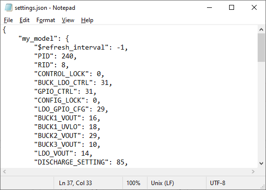
- Click File > Save Settings in the top left
corner of the GUI. This exports the register settings in a JSON file that is
provided to generate the NVM spin.
 Figure 6-9 Example Settings Output