SLVUBQ1A August 2020 – May 2021 TPS543620
- Trademarks
- 1Introduction
- 2Configurations and Modifications
-
3Test Setup and Results
- 3.1 Input/Output Connections
- 3.2 Efficiency
- 3.3 Output Voltage Regulation
- 3.4 Load Transient and Loop Response
- 3.5 Output Voltage Ripple
- 3.6 Input Voltage Ripple
- 3.7 Synchronizing to a Clock
- 3.8 Start-up and Shutdown with EN
- 3.9 Start-up and Shutdown with VIN
- 3.10 Start-up Into Pre-Bias
- 3.11 Hiccup Current Limit
- 3.12 Overvoltage Protection
- 3.13 Thermal Performance
- 4Board Layout
- 5Schematic and Bill of Materials
- 6Revision History
3.4 Load Transient and Loop Response
Figure 3-10 and Figure 3-11 show the response to load transients for both designs. The current step is from 1.5 A to 4.5 A and the current step slew rate is 1 A/µs. An electronic load is used to provide a DC 1.5-A load and the load transient circuit on the EVM is used to provide a 3-A step. The VOUT voltage is measured using TP10 for U1 and TP29 for U2.
When using the load transient circuit included on the TPS543620EVM, slowly increase amplitude of function generator for desired load step amplitude then vary the rise and fall times for the desired slew rate. The current for the load step can be sensed with the ISNS test point. The default resistors on the EVM provide a gain of 20 A/V. With this gain, a 3-A step will result in 150-mV at the ISNS test point.
To use the load transient circuit with U1, move R27 to R28.
Figure 3-12 and Figure 3-13 show the loop characteristics for both designs. Gain and phase plots are shown for VIN voltage of 12 V and a 0.2-Ω resistive load.
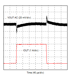 Figure 3-10 U1 Transient
Response
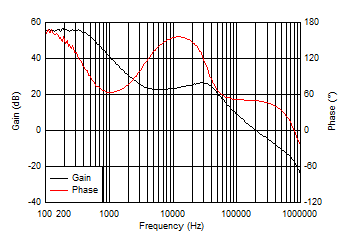 Figure 3-12 U1 Bode
Plot
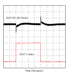 Figure 3-11 U2 Transient Response
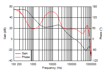 Figure 3-13 U2 Bode Plot
Figure 3-14 and Figure 3-15 shows the loop characteristics for U2 with the 3 different ramp settings.
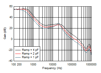 Figure 3-14 U2 Loop Gain with Different Ramp
Settings
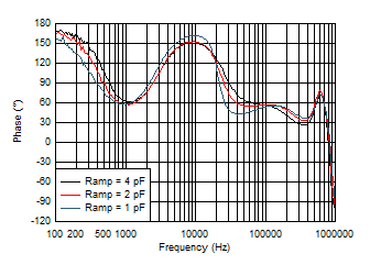 Figure 3-15 U2 Loop Phase
with Different Ramp Settings