SLVUBX2A August 2020 – March 2021 TPS62912 , TPS62913
4 Board Layout
This section provides the EVM board layout and illustrations in Figure 4-1 through Figure 4-6. The Gerbers are available on the EVM product page. Revision B of the PCB just added a pin 1 indicator for the inductor, in the silkscreen, to ensure that the inductor is assembled with the lowest-noise polarity.
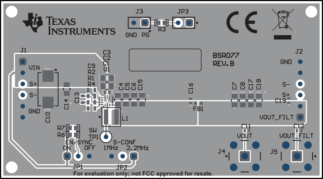 Figure 4-1 Top Assembly.
 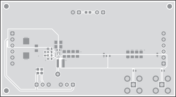 Figure 4-2 Top Layer.
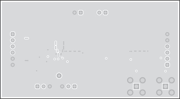 Figure 4-3 Internal Layer 1 .
 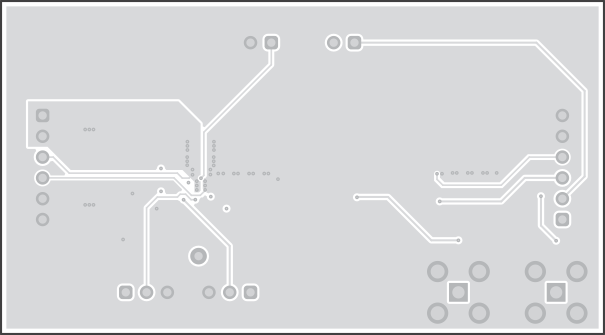 Figure 4-4 Internal Layer 2.
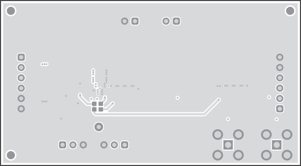 Figure 4-5 Bottom Layer .
 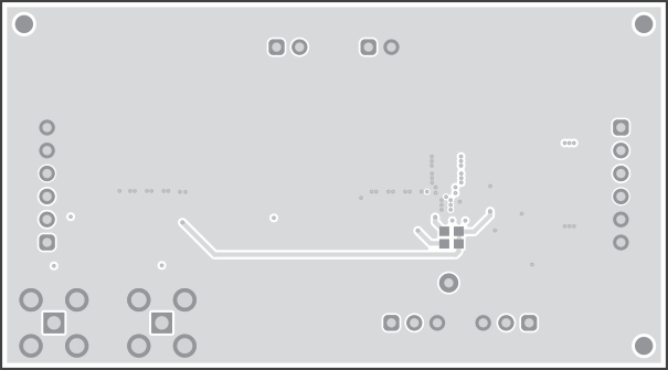 Figure 4-6 Bottom Layer (Mirrored).