SNAU264 July 2021 CDCDB800
3.1 Setup Procedure
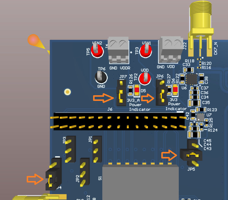
- Verify the jumpers match the states shown in Table 3-1 to reflect the default output clock interfaces configured on the EVM.
 Figure 3-2 Default Jumper Configuration.
 - Connect a 3.3-V to 5-V power supply to VDD and VDD_R as well as associating GND terminals of the 2 power blocks. This powers the on-board LDO regulator to supply 3.3 V to the VDD and VDDR rails of the IC. Both VDD and VDDR have associated '3V3' and '3V3_A' LEDs that should be lit red when ON.
Set the desired clock output using the output selection control switches, S1[1:7], as seen in Table 3-1.
Table 3-1 DIP Switch SelectionSelected Output S1 Pin Default Setting
OE1# 1 ON
OE2# 2
OFF
OE3#
3
OFF
OE4#
4
ON
OE5#
5
OFF
OE6#
6
OFF
OE7#
7
OFF
CKPWRGD_PD#
8
ON
- Connect and measure any clock output SMA labeled CKx_P or CKx_N to an oscilloscope or other test instrument using SMA cable(s). The output clock will be a level-translated/buffered copy of the selected clock input.Note: Populated output clocks are DC-coupled to the SMA connectors.Note: Any active output trace(s) without proper load termination can cause signal reflections on the board, which can couple onto nearby outputs and degrade signal quality and measurement accuracy. To minimize these effects, be sure to properly terminate any unused output trace with a 50-Ω SMA load, or else disconnect any unused output trace from the device output pin by removing the series 0-Ω resistor. An unused output or output bank may also be disabled using the output mode control switch.