SNIA043A july 2021 – april 2023 TMP114 , TMP144
4.2 Designing an Under-Component Layout With the TMP114 Temperature Sensor
Figure 4-3 shows a 3D rendering of the TMP114 temperature sensor underneath the IWR6843 integrated single-chip mmWave sensor. The IWR6843 mmWave sensor was selected for under-component sensing here because of the footprint, available vertical clearance, and integrated self-calibration over temperature.
 Figure 4-3 Board Rendering of TMP114 Temperature Sensor Underneath IWR6843 Sensor
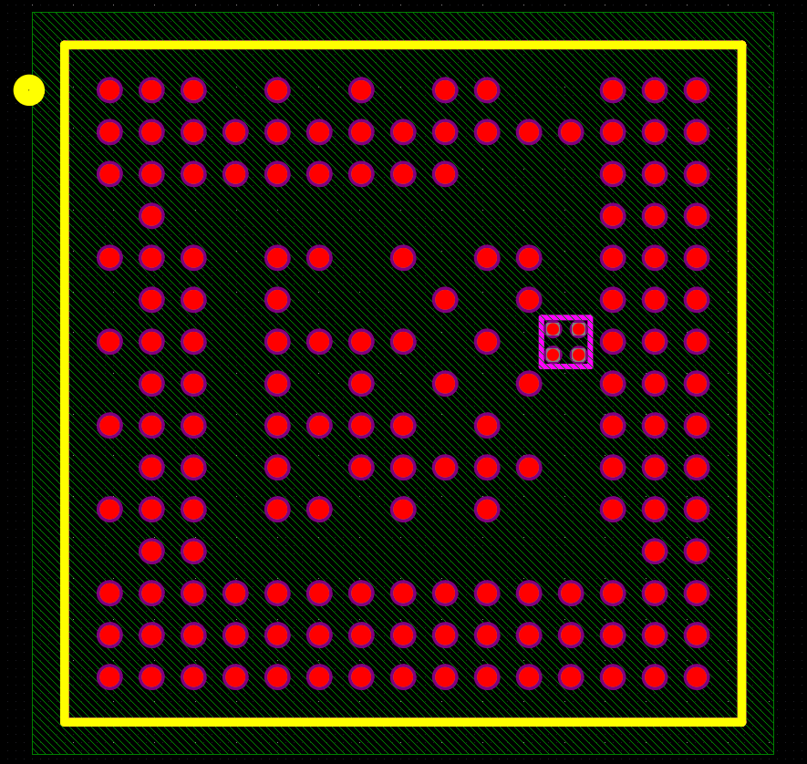
When deciding if an under-component approach is appropriate, one of the most important factors is that there is room in the footprint for the sensor to be placed. Not all components and processors meet this requirement; therefore, use another method of temperature monitoring. The IWR6843; however, is available in a Flip Chip Chip-Scale Package (FCCSP) which includes adequate spacing between the solder balls for the TMP114 temperature sensor footprint as shown in Figure 4-4.
 Figure 4-4 IWR6843 and TMP114 Footprints
Rendered in PCB Editor
Figure 4-4 IWR6843 and TMP114 Footprints
Rendered in PCB EditorVertical clearance must also be enough for the sensor to fit entirely. With the IWR6843, there is plenty of vertical clearance due to the height of the solder balls being much higher than the height of the TMP114 temperature sensor package.
 Figure 4-5 TMP114, TMP144, and IWR6843 Vertical
Dimensions
Figure 4-5 TMP114, TMP144, and IWR6843 Vertical
DimensionsThere are several tradeoffs to this kind of temperature sensing placement. For instance, an under-component strategy for temperature sensing can increase board cost, because smaller diameter in-pad vias are required to route the communication lines from the temperature sensor. When placing the sensor under a leaded package component, additional cost can still be seen if a lower minimum trace width is required for routing. Assembly costs can also be higher, as a second reflow is needed to allow the sensor to be placed first, followed by the component to be placed on top.