SNIA044 November 2021 TMP61 , TMP61-Q1 , TMP63 , TMP63-Q1 , TMP64 , TMP64-Q1
3.2 Three-Point Differential Temperature Measurement
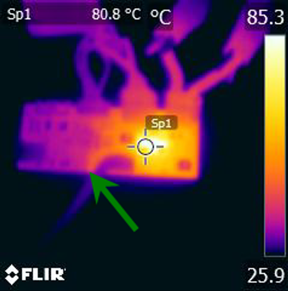
In this example of differential temperature measurements, a TIDA-00982 2S1P Drone BMS Board is used. The ground plane on layer 2 functions as the heatsink on a 4-layer PCB. The thermal power pad of the IC is soldered to the PCB copper pad on layer 1 and 12 vias are used to connect to the ground plane on layer 2 of the PCB. The thermal conduction of the ground plane on layer 2 results in good thermal flow to measure the temperature differentially external to the IC. The thermal flow across the PCB is shown in the thermal image in Figure 3-4.
 Figure 3-4 Thermal Flow Across TIDA-00982 Ground Plane
Three points on the PCB are used in the differential measurements: the die hot spot (Sp1) and two reference points (Sp2 and Sp3). In Figure 3-5, a thermal image of the PCB is shown at nominal operation with the 3 temperature measurements, along with an equivalent thermal circuit.
Using these measurements, the temperature drops (DT1 and DT2) between the test points are calculated, which are then used to determine the ratio of the two temperature drops. The measurements and calculations are summarized in Table 3-1.
| Reference Point | Temperature | Calculation | Value | Description |
|---|---|---|---|---|
| Sp3 | 27.6°C | DT2 | 8.9°C | Sp2 – Sp3 |
| Sp2 | 36.5°C | DT1 | 30.8°C | Sp1 – Sp2 |
| Sp1 (Die) | 67.3°C | Ratio | 3.46 | DT1 / DT2 |
Using the ratio of the temperature drops, the die temperature (Sp1) can now be calculated from only the temperature measurements at the two reference points, Sp2 and Sp3. For example, consider another thermal IR image of the same PCB under heavy operation in Figure 3-6, along with the equivalent thermal circuit. Assume that initially Sp1 is unknown.
To determine the die temperature, the temperature drop from Sp2 to Sp3 (DT2) is found. Then, the temperature drop (DT1) from Sp1 to Sp2 is calculated by multiplying DT2 by the previously determined ratio of 3.46. Adding DT1 to Sp2 gives the calculated die temperature (Sp1). These calculations are summarized in Table 3-2. As Figure 3-6 shows, the actual measured die temperature (Sp1) is 90.1°C, and the calculated die temperature from the differential measurements is 89.3°C. The differential temperature error in this test case is –0.8°C.
| Reference Point | Measured Temperature | Calculation | Temperature | Description |
|---|---|---|---|---|
| Sp3 | 45.6°C | DT2 | 9.8°C | Sp2 – Sp3 |
| Sp2 | 55.4°C | DT1 | 33.9°C | DT2 × Ratio |
| Sp1 | 90.1°C | Die Temperature | 89.3°C | Sp2 + DT1 |
Therefore, using this differential temperature measuring technique and a thermal camera, the die temperature of an IC can be calculated within ±1°C. Using two of TI’s TMP6 thermistors and a dedicated thermal layout, measuring the die temperature can be performed accurately.