SNOA930C March   2015  – May 2021 LDC0851 , LDC1001 , LDC1001-Q1 , LDC1041 , LDC1051 , LDC1101 , LDC1312 , LDC1312-Q1 , LDC1314 , LDC1314-Q1 , LDC1612 , LDC1612-Q1 , LDC1614 , LDC1614-Q1 , LDC2112 , LDC2114 , LDC3114 , LDC3114-Q1


  1.   Trademarks
  2. 1The Sensor
    1. 1.1 Sensor Frequency
    2. 1.2 RS and RP
      1. 1.2.1 AC Resistance
      2. 1.2.2 Skin Effect
  3. 2Inductor Characteristics
    1. 2.1 Inductor Shape
      1. 2.1.1 Example Uses of Different Inductor Shapes
    2. 2.2 Number of Turns
    3. 2.3 Multiple Layers
      1. 2.3.1 Mutual Inductance of Coils in Series
      2. 2.3.2 Multi-Layer Parallel Inductor
      3. 2.3.3 Temperature Compensation
    4. 2.4 Inductor Size
    5. 2.5 Self-Resonance Frequency
      1. 2.5.1 Measurement of SRF
      2. 2.5.2 Techniques to Improve SRF for Wire-wound Inductors
  4. 3Capacitor Characteristics
    1. 3.1 Capacitor RS, Q, and SRF
    2. 3.2 Effect of Parasitic Capacitance
      1. 3.2.1 Recommended Capacitor Values
    3. 3.3 Capacitor Placement
  5. 4Physical Coil Design
    1. 4.1 Example Design Procedure Using WEBENCH
      1. 4.1.1 General Design Sequence
    2. 4.2 PCB Layout Recommendations
      1. 4.2.1 Minimize Conductors Near Sensor
      2. 4.2.2 Sensor Vias and Other Techniques for PCBs
  6. 5Summary
  7. 6References
  8. 7Revision History

Multi-Layer Parallel Inductor

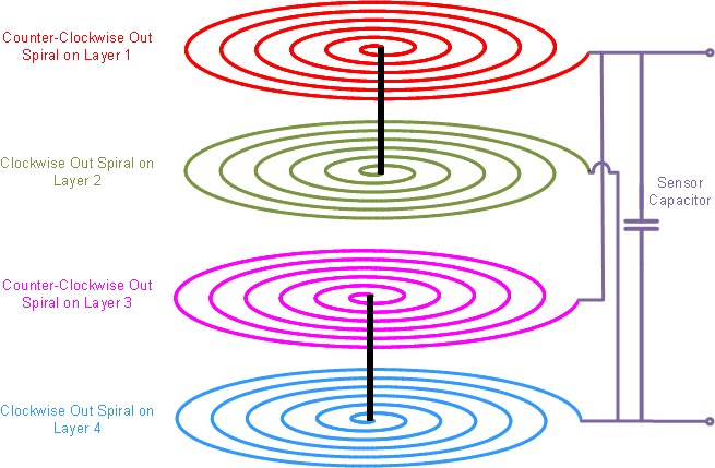
Minimizing the RS is necessary to obtain the highest resolution RP measurements. This also improves the L measurements for the LDC161x and LDC131x devices. With four or more layers users can start using the parallel coil structure shown in Figure 2-9 and Figure 2-10 to lower RS. This design may be useful for some applications which need to optimize RP measurements.
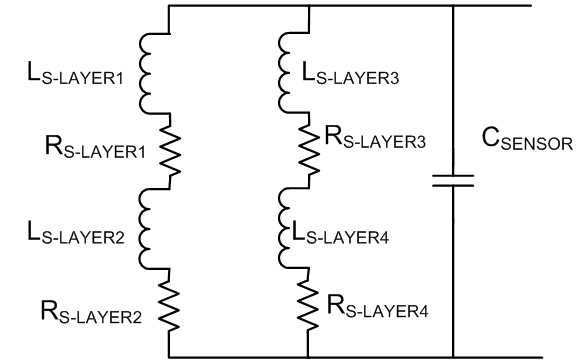
GUID-5139A46E-AC26-497E-86D6-3BA99552FF5F-low.gifFigure 2-9 Multi-layer Parallel Coil Schematic
GUID-9D0C85A5-EADC-4B68-8D3B-C0B2F2E7CF87-low.gifFigure 2-10 Multi-layer Parallel Inductor