SNOA949 May 2016 LDC1312 , LDC1312-Q1 , LDC1314 , LDC1314-Q1 , LDC1612 , LDC1612-Q1 , LDC1614 , LDC1614-Q1
2.1 Operational Parameters That Affect Duty Cycling
The multi-channel LDC family of devices has 2 and 4 channel versions. When configured to sample on multiple channels, the LDC sequentially samples the channels. Figure 1 and Figure 2 show both single channel and multichannel mode sequencing in continuous conversion of the LDC, representing a non-duty cycled mode of operation. The normal sequence of tasks on each channel include sensor activation, conversion, channel switching (multi-mode only), and data readback.
 Figure 1. Single-Channel Mode Sequencing In Continuous Conversion
  Figure 2. Multi-Channel Mode Sequencing In Continuous Conversion
 The sum of the times it takes for each task to complete is equivalent to a sample time, during which the device needs to be actively running. In the data sheet this is referred to as normal mode. In the remainder of this applications note this will be referred to as active mode. We will also distinguish between sampling period (TS) and sampling time (tN). The former is defined as the time between consecutive samples on the same channel, and the latter is defined as the time required to obtain a single sample. This is expressed in Equation 1 where tN is the time the device spends sampling in active mode.
- tN is the time the device spends sampling in active mode
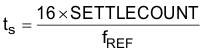
- tS is the sampling time
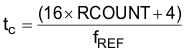
- tC is the conversion time
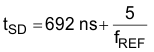
- tSD is the switch-delay time
- tRB is the data readback time
where
In general, tSD < tS << tC. Consequently, tC has the most impact on sampling time and hence, duty cycle.
The sensor activation time, tS, refers to the amount of time needed for the sensor oscillation to startup and stabilize. This activation time (tS) is programmable via the SETTLECOUNT register for each channel and given by Equation 2.
- fREF is the reference clock frequency
where
The sensor conversion time, tC , is the largest part of this sequence. It represents the number of reference clock cycles (RCOUNT*16) used to perform a measurement conversion. As seen in Equation 3, the sensor conversion time can be set by the RCOUNT register value for each channel.
The choice of RCOUNT value is driven by the resolution required by the application. If the required resolution is N bits, then Equation 4 can be used to calculate an initial value for RCOUNT:
See either section 7.3.2 of the LDC1614 data sheet (SNOSCY9) or other application notes (SNOA944, SNOA945) for a more thorough explanation of RCOUNT and sample resolution.
When the LDC is in multichannel mode, the channel switch delay needs to be included in the total sampling time. This is the delay time between the end of a sensor conversion on one channel and the beginning of sensor activation on a subsequent channel. This delay time is relatively minimal and is given by Equation 5:
In addition to the time required to complete the three tasks discussed above, the microprocessor takes some time to read back the channel measurement. This data readback time, tRB, is a function of the data resolution, the number of data registers being read, the number of clocking cycles to read or write to each register, and the I2C data rate.
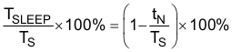
The total time to complete this sequence is the total amount of time for which the LDC must be in active mode (Equation 1). If fS is the required sampling rate and TS is the sampling period (TS=1/fS), the idea behind the duty-cycling technique is that the device is put into sleep mode when it is not operating in this data conversion process (TSLEEP= TS - tN). Consequently, the percentage of time the LDC is in a low power sleep mode is given by Equation 6:
To place the LDC in sleep mode, write the value 1 to the CONFIG.SLEEP_MODE_EN register field. While in sleep mode, the LDC retains its register contents except for those in the data registers, which must be read before the device is placed in sleep mode. To exit sleep mode, write the value 0 to the CONFIG.SLEEP_MODE_EN register field.
For more information on how to configure the multichannel LDCs, refer to either the LDC131x data sheet or the LDC161x data sheet.
In summary, given a minimum sampling rate required by the application, the duty cycle only needs to be large enough to meet the minimum resolution requirements of the application. Figure 3 illustrates this graphically.
 Figure 3. Duty Cycle as a Function of Settling Time, Conversion Time, Switching Time, and Readback Time
 One other thing to note is that there is also a maximum limit to how fast the sampling rate can be while still allowing for duty-cycling. For example, if the application requires a high resolution where RCOUNT is 65535, then tN is around 25 ms. In order for duty-cycling to work, TS must be greater than tN, otherwise TSLEEP will be less than 0. Therefore, the sampling rate cannot be more than 40 SPS. Figure 4 shows the maximum sampling rate allowed for various RCOUNT values
 Figure 4. Maximum Achievable Sampling Rates for Various RCOUNT Values