SNOAA68 June 2021 LMG3410R050 , LMG3410R070 , LMG3410R150 , LMG3411R050 , LMG3411R070 , LMG3411R150 , LMG3422R030 , LMG3422R050 , LMG3425R030 , LMG3425R050 , LMG3522R030-Q1 , LMG3526R030
3 Addressing GaN Failure Mechanisms
Failure mechanisms are present in all devices. Reliability engineering consists of making devices robust to failure mechanisms and their resulting failure modes. For GaN devices, the major failure modes are the increase of leakage currents and changes in parameters such as on-resistance. These can result in a reduction in efficiency or in circuit malfunction. Hard-failure can also occur.
In GaN devices, the primary failure mechanisms are
Time Dependent Breakdown (TDB), hot-carrier degradation,
and charge trapping. Time Dependent Breakdown is a
well-known phenomenon(13) in dielectrics used in silicon processing, and its
modeling is treated in JEDEC publications(14). It occurs due to high electric-field and is
responsible for increased leakage currents and can lead to
hard-failure. Hot-carrier degradation is also well-known in Si
MOSFETs, where hot-carrier stress causes defect generation.
Hot-carriers are created by hard-switching in power FETs, and have
been seen to result in both charge trapping and wearout in GaN
FETs(5, 15).
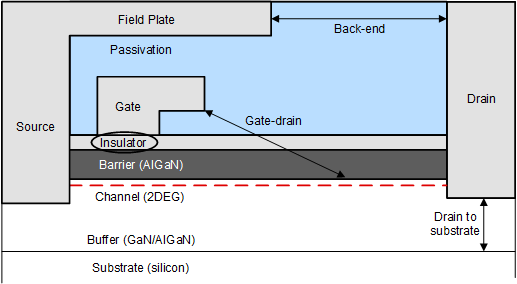
GaN FETs operate with high electric fields in several regions, as shown in Figure 3-1. TI GaN FETs have been engineered for TDB lifetime with the use of special test structures for each of these high-field regions. A model has been built incorporating 1.8 million device hours of testing and shows a low FIT rate of 0.8 FIT with 10 years of continuous application of 480 V and 125°C for the LMG3410R070 product.
 Figure 3-1 Schematic
cross-section of the GaN device showing the high-field
regions in the device.
Figure 3-1 Schematic
cross-section of the GaN device showing the high-field
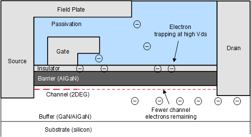
regions in the device.Charge trapping is also a well-known phenomenon in semiconductor devices, and can cause parametric shifts. An important consequence of charge trapping in GaN devices is a shift in the on-resistance, RDS(ON)(16). Negative trapped charge repels channel electrons, thereby resulting in fewer electrons in the channel, as shown in Figure 3-2. RDS(ON) increases because the number of electrons in a portion of the channel layer is reduced. Charge can be trapped in the buffer layer, in dielectrics, and at interfaces. Charge trapping can occur due to high drain voltage when the device is off, or from hot electrons when switching. The RDS(ON) inclusive of charge trapping effects is called dynamic RDS(ON). The dynamic nature arises because RDS(ON) recovers as the trapped charge dissipates or detraps. It is therefore important to evaluate dynamic RDS(ON) at the timescales of switching cycles. A consequence is that if the detrapping or device on-time is low, there could be more charge buildup. Dynamic RDS(ON) evaluation at low duty cycle is therefore a good method to validate material quality.
Power devices need to be engineered for stable RDS(ON), since they are continually subject to high voltage and hot electron generation while switching. Increases in RDS(ON), will decrease efficiency through higher conduction loss. Furthermore, the trap density can increase as the device ages. It is therefore important for dynamic RDS(ON) to be stable with aging, to prevent excessive self-heating and premature failure.
 Figure 3-2 Schematic
cross-section of a GaN device shows how trapped electrons
can increase RDS(ON) by reducing the number of
electrons in the channel layer
Figure 3-2 Schematic
cross-section of a GaN device shows how trapped electrons
can increase RDS(ON) by reducing the number of
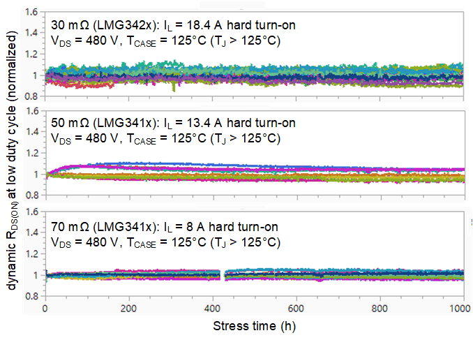
electrons in the channel layerTI GaN products have been engineered for stable dynamic RDS(ON) with aging. This was achieved through years of in-house material and process engineering. It included ways of growing high-quality GaN crystal, optimizing the dielectric films, and achieving very clean interfaces. We validate dynamic RDS(ON) lifetime stability by using the test vehicle in Figure 2-1. This is one of the circuits listed in JEP182 for the continuous-switching evaluation of GaN power conversion devices. Hard-switching stress is applied per JEP180 at a current corresponding to the maximum power condition, the maximum recommended VDS and worst-case junction temperature, for 1000h. Dynamic RDS(ON) stability with aging is validated through low duty-cycle hard-switching stress. Dynamic RDS(ON) aging data from products in the LMG34xx family is shown in Figure 3-3. The duty cycle used was about 0.5%, which provides excellent ability to discriminate material quality. Dynamic RDS(ON) measurement is conducted per JEP173. The high stability of dynamic RDS(ON) under very low duty cycle for best-practice lifetime stress conditions attests to excellent aging of the material: it demonstrates the lack of new trap creation with aging and validates the long-term stability of dynamic RDS(ON) under all conditions of operation. To assure manufacturability of material with this quality, we have had a coordinated program to develop in-line electrical tests that are predictive of dynamic RDS(ON) in application. The excellent dynamic RDS(ON) stability of our production material has also been verified by others(16).
The reason that low duty cycle provides excellent sensitivity to charge trapping is because the device spends most of its time at high-voltage and the small on-time limits de-trapping(16, 17). This gives the corresponding dynamic RDS(ON) parameter excellent sensitivity to material quality. The increased sensitivity of dynamic RDS(ON) to detect trapping helps it pick up less electrically active traps. This is consequential because these latent or nascent defects would become more electrically active as they age and later start affecting dynamic RDS(ON) for operation at regular duty cycles. Dynamic RDS(ON) under low duty cycle thereby provides an early detection method for the effects of aging. Stable dynamic RDS(ON) under low duty cycle stress shows that these latent traps are not a concern.
We also evaluated dynamic RDS(ON) stability under two other modes of operation in power supplies. First is under prolonged off-state conditions by applying off-state stress at a temperature of 125°C and VDS = 500 V. The dynamic RDS(ON) is measured in situ every 10 minutes with the results plotted in Figure 3-4, and shows stable behavior with aging. Second is under Dynamic High Temperature Operating Life (DHTOL) operation per JEP180 under both hard and soft-switching operation. The parts had stable efficiency, as described later in section 8, which validates dynamic RDS(ON) stability. The stable behavior under these conditions further provides assurance that TI GaN technology is natively robust to charge trapping mechanisms.
 Figure 3-3 Dynamic
RDS(ON) is stable under low duty-cycle
hard-switching best-practice stress conditions. Parts were
run at 15–21 kHz with a duty cycle of about 0.5%. The
stability demonstrates lack of new trap creation and attests
to the excellent material quality. Dynamic
RDS(ON) is measured per JEP173
 Figure 3-4 Dynamic
RDS(ON) is stable under off-state high
voltage and temperature conditions, providing further
assurance that TI GaN is robust to charge trapping
mechanisms. The stress was applied using the circuit of
Figure 2-1 with IL = 0 A.
Figure 3-4 Dynamic
RDS(ON) is stable under off-state high
voltage and temperature conditions, providing further
assurance that TI GaN is robust to charge trapping
mechanisms. The stress was applied using the circuit of
Figure 2-1 with IL = 0 A.An important difference between GaN and Si FETs is the mechanism causing breakdown. The drain breakdown voltage of Si power FETs is limited by impact ionization, resulting in their voltage rating being limited by avalanche breakdown. As a result, Silicon power FETs do not have much headroom above their voltage rating for transient events. GaN has avalanche(18) capability, but its three-times larger bandgap, allows it to better withstand higher fields without avalanching. The voltage rating of GaN FETs is typically lower than the avalanche limit of the material, giving them transient voltage capability. This aspect allows them to switch through surge without avalanching, as is discussed later.
Finally, it is important to address the effects of current flow at high voltage. Current flows at high voltage during hard-switching in any power device, as explained in reference 5. There are two relevant effects. Firstly, current flow at high voltage creates hot carriers. Their higher energy enables them to scatter into a larger volume, which can result in more charge trapping and cause an increase in dynamic RDS(ON). Hot carriers can also cause wear out or degradation due to defect generation. Current flow at high voltage can also exercise safe operating area (SOA) boundaries, for which the part needs lifetime reliability. TI GaN is robust to failure modes arising due to hot carriers. As shown in Figure 3-3, we validate long-term dynamic RDS(ON) stability at stringent low duty-cycle operation under hot-carrier creating hard switching conditions. The hard-switching lifetime and SOA aspects are discussed later.