SNOAA68 June 2021 LMG3410R050 , LMG3410R070 , LMG3410R150 , LMG3411R050 , LMG3411R070 , LMG3411R150 , LMG3422R030 , LMG3422R050 , LMG3425R030 , LMG3425R050 , LMG3522R030-Q1 , LMG3526R030
2 Background
The qualification standards in use for silicon were first published in the 1990’s. The popular JEDEC JESD47 standard(2), “Stress-Test-Driven Qualification of Integrated Circuits” was first published in July 1995 and the Automotive Electronics Council (AEC) Q100(3) was first published in June 1994. These standards specify many tests which may be classified into three categories: device, electrostatic discharge (ESD), and package. At the time, memory and logic were the predominant applications, and the accelerated bias tests were intended to achieve an electric-field equivalent lifetime. The switching transitions of power management applications were not specifically considered.
Traditional device qualification is run by using a 1000h test at a junction temperature of 125ºC or higher at the maximum operating voltage. Running at 125ºC is equivalent to about nine years of use at Tj = 55ºC using an assumed activation energy of 0.7 eV.
Many of the tests also require a large number of parts to obtain defectivity and failure in time (FIT) statistics. For further background on traditional silicon qualification, see references 4 and 5.
Although JEDEC specifies the need for dynamic testing, conditions are not prescribed due to the ever-evolving applications and material sets in our industry(6). The field of power conversion illustrates the difficulties. There are many different topologies and numerous components with which the GaN FET interacts. Determining the lifetime of a GaN FET in a power converter is challenging for the following reasons. First, running acceleration studies could cause many non-GaN failures. Second, the applicability to different topologies would not be clear. Third, the energy usage of running the large number of power converters needed is large. It has therefore not been straightforward to assure product-level reliability in a broad sense. As a result, traditional reliability testing has not covered the switching conditions of power management.
The need for GaN-specific reliability validation arose because traditional silicon qualification methodology was not fully addressing application reliability for GaN products. During the early days, we observed that hard-switched transitions were causing overheating and occasional hard-failure. This finding is important because a broad class of power conversion applications are hard-switched. We developed a comprehensive methodology for qualifying the reliability of GaN products, described in references 4 and 5. The papers describe a common approach of validating the application reliability of GaN FETs for a broad class of applications.
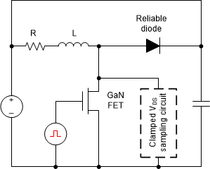
 Figure 2-1 Schematic of
the test vehicle used for universal hard-switch reliability
validation of TI GaN devices. Dynamic RDS(ON) is
measured using the clamped VDS sampling
circuit.
Figure 2-1 Schematic of
the test vehicle used for universal hard-switch reliability
validation of TI GaN devices. Dynamic RDS(ON) is
measured using the clamped VDS sampling
circuit.The common approach is enabled by use of the switching locus curve to represent the type of switching stress applied to the device, and thereby the failure mechanism exercised. The switching locus curve is the trajectory of the iD-vDS waveform during a switching cycle(7). A test vehicle circuit with a hard-switching locus will therefore apply relevant stress for hard-switching applications(7).
Our test vehicle circuit shown in Figure 2-1 and described in references 4 and 5, is a boost converter stage with the output tied to the input to conserve energy. It is a similar circuit to the double pulse tester (DPT) with a different control. We use it in continuous-pulse mode for providing accelerated hard-switching stress per JEP182(8). A highly-reliable diode is used for the high-side device, eliminating high-side drive complexity. Its simplicity minimizes system-related failures, enabling accelerated testing for the desired failure mechanism. It is also designed to measure dynamic RDS(ON) per JEP173(9).
Traditional silicon qualification testing alone is not a guarantee for reliable application performance because it does not include hard-switching transitions, nor does it test for dynamic RDS(ON). Both aspects are very important for the proper operation of all devices in hard-switching applications. We have seen that GaN devices from processes that pass traditional silicon qualification can still overheat and show a decrease in efficiency when run in a in a hard-switched application. However, parts run reliably if the process passes traditional qualification testing plus hard-switching reliability testing(10).
It is often asked whether a device that is robust to hard-switching is also robust for soft-switching applications. This is reasonable thinking because hard-switching creates more hot electrons, which can increase electron trapping and result in higher dynamic RDS(ON)(11). It was previously shown(10) that hard-switching is the more stressful case for TI GaN devices. However, there have been recent literature reports(12) that soft-switching can cause higher dynamic RDS(ON) for some types of devices. Our stress testing confirms that TI GaN devices are reliable for both hard and soft-switching applications and confirms that soft-switching does not cause higher dynamic RDS(ON) for GaN technology in general.