SNOAA73 May 2021 LMP2012QML-SP , LMP7704-SP , TPS7A4501-SP
Design Steps
See the Design References section for an Excel calculator that calculates the resistor values for the required specifications.
- Define the input voltage range for the circuit. For this design Vin_min = 0 V, Vin_max = 5 V is chosen.
- Define the output current range for the circuit. For this design Iout_min = 4 mA, Iout_max = 20 mA is selected.
- Calculate R7 and R8 to set the output voltage for the TPS7A4501-SP LDO. The equation to set the output voltage for this adjustable LDO follows:
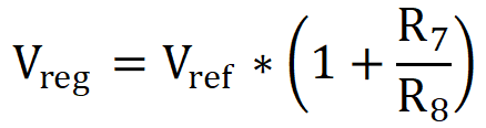
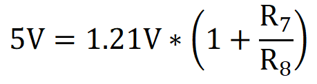
In this equation, Vref is the internal bandgap reference voltage for the LDO. TPS7A4501-SP has a nominal reference voltage Vref = 1.21 V and this design is targeting Vreg = 5 V, so the following applies:
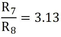
To choose values, the following guideline is used: The current in the feedback resistors from output to ground of an LDO must be at least 100 times the leakage current into the ADJ pin to avoid output accuracy issues. For TPS7A4501-SP, the leakage current of the ADJ pin is 3 μA (typ). This yields the following inequality:
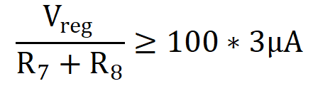
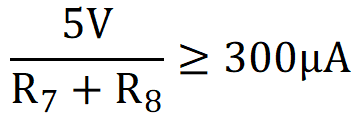 16.67 kΩ ≥ R7 + R8
With R8 = 3.97 kΩ (standard value), the following equation is true:
R7 = 3.97 kΩ * 3.13 = 12,426 Ω ≈ 12.4 kΩ (standard value)With these values for R7 and R8, the following equation is valid:
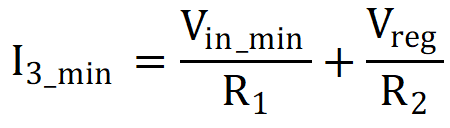
R7 + R8 = 3.97 kΩ + 12.4 kΩ = 16.37 kΩ ≤ 16.67 kΩNote: Since this design has a current budget limitation, it is desirable to size R7 and R8 to be near the limit to minimize this quiescent current contribution. - Define the minimum and maximum currents through R3. See Design Note #5 before defining these currents. For this design, I3_min = 20 μA, I3_max = 100 μA, is chosen.
- Calculate the values for
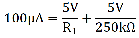
R1 and R2 to set I3_min and
I3_max as defined in Design Step #4. To do this, use the first equation along with the specifications for Vreg,
Vin_min, Vin_max, I3_min and
I3_max. When Vin = Vin_min, the following
equations occur:
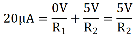 R2 = 250 kΩ (standard value)
When Vin = Vin_max, the following is true:
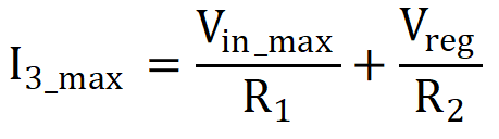
 R1 = 62.5 kΩ ≈ 62 kΩ (standard value)
 - Calculate R3 / R4 to set the required current gain. To do this, use this equation along with Iout_min and I3_min.
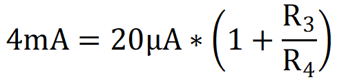
 Note: Only the minimum values of Iout and I3 are required to calculate R3 / R4 because it is assumed that Design Note #5 has been followed.
 - Choose values for R3 and R4. Sizing R3 is much less important than sizing R4 because headroom issues can arise if care is not taken when sizing R3. To see why, analyze the nodal voltages under the maximum loading condition, Iout = Iout_max = 20 mA. The load voltage is the following:Vload = Iout_max * Rload = 20 mA × 250 Ω = 5 V
Most of the output current comes through R4, so with R4 = 100 Ω, the voltage at Iret is approximately:
5 V + 100 Ω * 20 mA = 7 V
Vreg is referenced to Iret, so relative to the supply ground, Vreg = 7 V + 5 V = 12 V, in which case the LDO enters dropout. If the LDO enters dropout, the LDO loses its power supply rejection (PSR) properties, and the op amp has a reduced positive supply and so has a reduced ability to drive the base of the transistor to provide additional output current. Furthermore, if Vreg droops, the current through R3 will be reduced and the circuit begins to exhibit non-linear behavior. Also, if R6 is too large, the additional voltage drop across R6 further reduces the available headroom for the transistor.
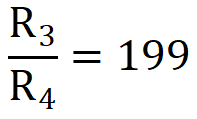
With these considerations in mind, choose R4 = 50 Ω to avoid problems with headroom. It follows that:
R3 = 199 * 50 Ω = 9.95 kΩ ≈ 9.88 kΩ (standard value)