SNOAA79 June 2021 DAC121S101QML-SP , LMP7704-SP , TPS7A4501-SP
Design Steps
Component Selection
- Identify the current sink
specifications:
- Specifications for the
circuit shown:
- Input voltage range (DAC output): 0mV to 500mV
- Resistive load: 15Ω
- Load current range: 0mA to 200mA
- Current error: ±4mA
- Specifications for the
circuit shown:
- Sense resistor selection
(RSense):
- The selection of
RSense comes down to power dissipation versus
precision.
- Smaller values of RSense yield smaller voltage drops for the same amount of current and ultimately dissipate less power. However, since the RSense voltage drop is smaller, higher precision components may need to be used to achieve the same error tolerance.
- Higher values of RSense can be created by paralleling resistors to share the power dissipation.
- In the circuit shown, the
RSense value is selected based on the maximum DAC output
voltage (VDACMax) and the maximum load current
(IMax) as shown:
- In this case, the 2.5-Ω
RSense produces a voltage of 10mV per 4mA of load
current. Therefore, to meet the desired current error specification of
±4mA, the total voltage error should be less than 10mV (2.5Ω × 4mA). The
total voltage error includes the offset voltage error from the op amp,
the op amp input bias current error through resistor RF, DAC output
error, and the RSense resistor error.
- Fortunately, the
LMP7704-SP has great DC performance
with a typical offset voltage of ±32µV and a typical input bias
current of ±0.2pA. Calculate the error contribution as follows:
- The DC error of the amplifier, as shown, is not a significant contributor to the allowed 10mV of error.
- In many cases, most of the error is observed from the RSense tolerance, RSense drift, and the DACs offset error, gain error, and drift.
- Use the DAC121S101QML-SP to achieve the circuit requirements and maintain the radiation performance.
- Fortunately, the
LMP7704-SP has great DC performance
with a typical offset voltage of ±32µV and a typical input bias
current of ±0.2pA. Calculate the error contribution as follows:
- The selection of
RSense comes down to power dissipation versus
precision.
- Amplifier selection
(U1A):
- The amplifier selection is rather straightforward. From the perspective of meeting the current error specifications, consider the offset voltage of the op amp and its input bias current (as shown previously in the Sense Resistor Selection section).
- The op amp should also have an input common-mode range that extends to the negative rail (GND in this case) to support the low output range of the DAC. However, there is a hidden criterion for selection under one or both of the following two conditions: (1) the MOSFET has a threshold voltage (VGS(th)) close to the available supply rail, (2) the resistive load of the system is close to the maximum load the supply rail can handle.
- The hidden criterion is the output voltage swing of the op amp. Looking the circuit, the selected MOSFET Q1 has a maximum VGS(th) across TID exposure of 4V and the circuit supply rail is 5V. At peak current, the source voltage of the MOSFET is at 0.5V which is also the voltage across RSense (200mA × 2.5Ω). In this case, the op amp with the 5-V supply must be able to swing to at least (V+) – 0.5V or 4.5V to reach VGS(th). Similarly, in the case of condition (2) the op amp must be able to swing close to the positive rail to maximize the largest resistive load that can be driven.
- Calculate the largest resistive load as follows (assuming no voltage
drop across Q1):
- MOSFET selection:
- Ensure that the MOSFET
VGS(th) can be driven by the op amp and that it can
handle the power dissipation for the expected load resistance and
maximum current:
- Ensure that the MOSFET
VGS(th) can be driven by the op amp and that it can
handle the power dissipation for the expected load resistance and
maximum current:
- Current Sink Control
Circuit
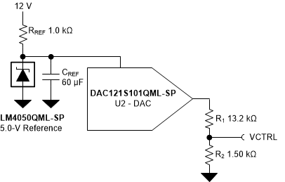
- The DAC121S101QML-SP can provide a means of adjusting the voltage used to control the current sink.
- The LM4050QML-SP provides a 5.0-V reference to the DAC. When CREF = 60μF, the LM4050QML-SP is immune to SETs.
- Since the DAC121S101QML-SP is a 12-bit DAC, it could have errors in the range of 10s of millivolts, which would dominate the system error. Therefore, the output voltage is scaled down by a factor of 5/49, given a maximum DAC operating voltage of 4.9V:
- Scaling down the voltage also means that any error introduced by the DAC121S101QML-SP or the LM4050QML-SP voltage reference are reduced by a factor of 5/49. Using a ratio of 5/49 also allows for the selection of standard 0.1% resistor values. The resistors introduce up to 0.179735% of error given the nominal resistor values and accounting for potential resistor value variation.
- A key consideration for
the system accuracy is the error introduced by the DAC and other
devices. The error is often referred to as the Total Unadjusted Error
(TUE) and is relative to the control voltage (VCTRL) which is
the dominant source of error for the circuit. In the circuit, the
following error sources must be considered:
- LM4050QML-SP 5.0-V Voltage Reference: Initial Accuracy, Drift over temperature (ΔVR/ΔT)
- DAC121S101QML-SP DAC: Zero Code Error (ZEC), Gain Error (GE), ZEC Drift, and GE Drift
- Resistor Divider (R1 and R2) Tolerance Error
- LMP7704-SP: VOS, IOS, and IBIAS
- In this circuit, both Beginning of Life (BOL) and temperature tolerances are considered for calculating the VCTRL TUE. Root Sum Square (RSS) is used to represent the added error of all sources. Error contributions from the voltage reference and the DAC are scaled by 5/49 in the TUE calculation.
DAC Data Sheet
SpecificationTUE
T= 25°CData Sheet
SpecificationTUE
ΔT = –55 to 125°CTUE + Gain Calibration
ΔT = –55 to 125°CINL (V)
2.75 LSB
3.357E-3
8.0 LSB
9.766E-3
9.766E-3
DNL (V)
0.21 LSB
256.348E-6
1.0 LSB
1.221E-3
1.221E-3
ZCE (V)
4 mV
4.000E-3
10 mV
10.000E-3
10.000E-3
ZCE-Drift (V)
–20 µV/°C
–3.6E-3
–3.600E-3
GE (V)
–0.11%
5.500E-3
1.00%
50.000E-3
1.221E-3
GE-Drift (V)
–1 ppm/°C
–900.0E-6
–900.000E-6
Volt. Ref.
Initial Acc. (V)
0.23% at IR<1mA
11.500E-3
0.23% at IR<1mA
11.500E-3
9.000E-6
ΔVR/ΔT (V)
34 ppm/°C
30.6E-3
30.600E-3
Op Amp
VOS (V)
±37 μV
37.000E-6
±500 μV
500.000E-6
500.000E-6
IBIAS (A)
±200 fA
200.000E-12
±400 pA
400.000E-12
400.000E-12
IBIAS × R2 (V)
300.000E-9
600.000E-9
600.000E-9
VOSDrift (V)
±5 μV/°C
900.000E-6
900.000E-6
Scaling Res.
Resistor Div.
898.674E-6
898.674E-6
898.674E-6
VCTRL RSS TUE (mV)
1.669E-3
6.420E-3
3.718E-3
VCTRL RSS Error%
0.334%
1.284%
0.744%
- The first TUE calculation does not include drift over temperature and achieves less than 1% accuracy. The next TUE calculation accounts for the variation in temperature for ΔT = 180°C (–55 to 125°C) as well as the extreme maximum and minimum values provided in each respective data sheet over temperature. Accounting for both extreme values as well as the effect of temperature drift on certain specifications, the second TUE calculation achieves less 2% TUE.
- In the previous calculation the error is dominated by the Gain Error (GE) of the DAC, which over temperature and radiation can vary as much as 1.0%. The GE accounts for up to 50mV of error at the output of the DAC or 5.102mV when scaled by a factor of 5/49. Reduce this error, as well as the error introduced by the initial accuracy of the reference, by performing gain calibration. With gain calibration, the TUE is reduced to 3.718mV or 0.759% of VCTRL. The calibration allows for the design to achieve 1.0% accuracy.
- Compensation components selection:
- Stability analysis is done in the frequency domain and circuit stability is verified by the small signal transient step response. The criterion to ensure stability is a minimum phase margin of 45 degrees or a rate-of-closure (ROC) of 20dB/decade at fcl (loop gain, AOLB = 0dB) where the AOL curve intersects 1/β.
- The following open-loop AC simulation breaks the loop at the input and the following equations are used to plot the relevant curves:
- The following figure shows the open-loop AC response of the circuit if Riso, RF, and CF are all zero (not in the circuit). The AOLB phase margin is 13.77° which indicates that the circuit is only marginally stable.
- Cin is the equivalent
input capacitance of the LMP7704-SP and is added due to the inductor L1 breaking the
interaction of AOLB with the amplifier input capacitance.
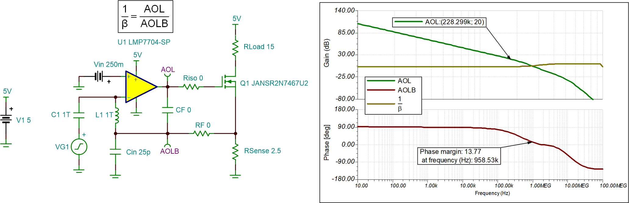
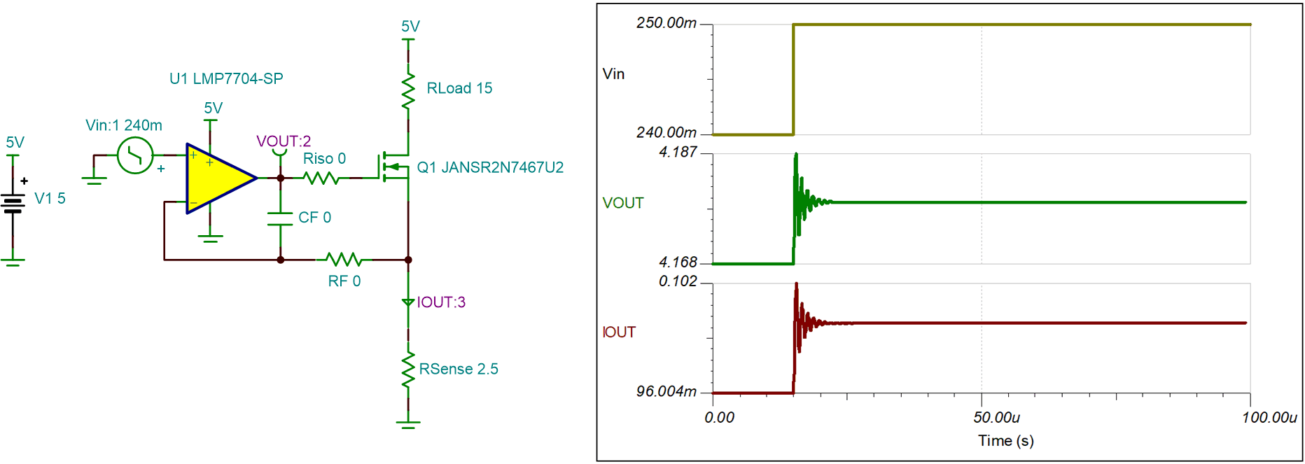
- The AC simulation can be
verified by the small signal step transient response. The small signal
transient step response shows that the circuit has a long settling time
with excessive ringing. Therefore, it is highly susceptible to
oscillations.
- The reason for the
instability is: the op amp output impedance interacts with the MOSFET
input capacitance and creates a pole in the AOL curve that causes a
40-dB/decade ROC. To compensate the circuit, start by finding the value
for the isolation resistor Riso, needed to mitigate the
problem. Two things are needed to find Riso, (1) the
frequency where AOL is 20dB (f20dBAOL), previously shown
in the figure as 228.3kHz, (2) the input capacitance of the
MOSFET which is found in the data sheet as 9.11nF. Then, use the
following equation:
- For more details on Riso and driving capacitive loads, see TI Precision Labs - Op Amps: Stability - Capacitive loads.
- The new open loop AC
response, after adding Riso, is shown next. Even though the
second pole in AOL was eliminated, the circuit remains only marginally
stable due to a zero in 1/β caused by the delay from Riso and
the input capacitance of the MOSFET in the V-I loop.
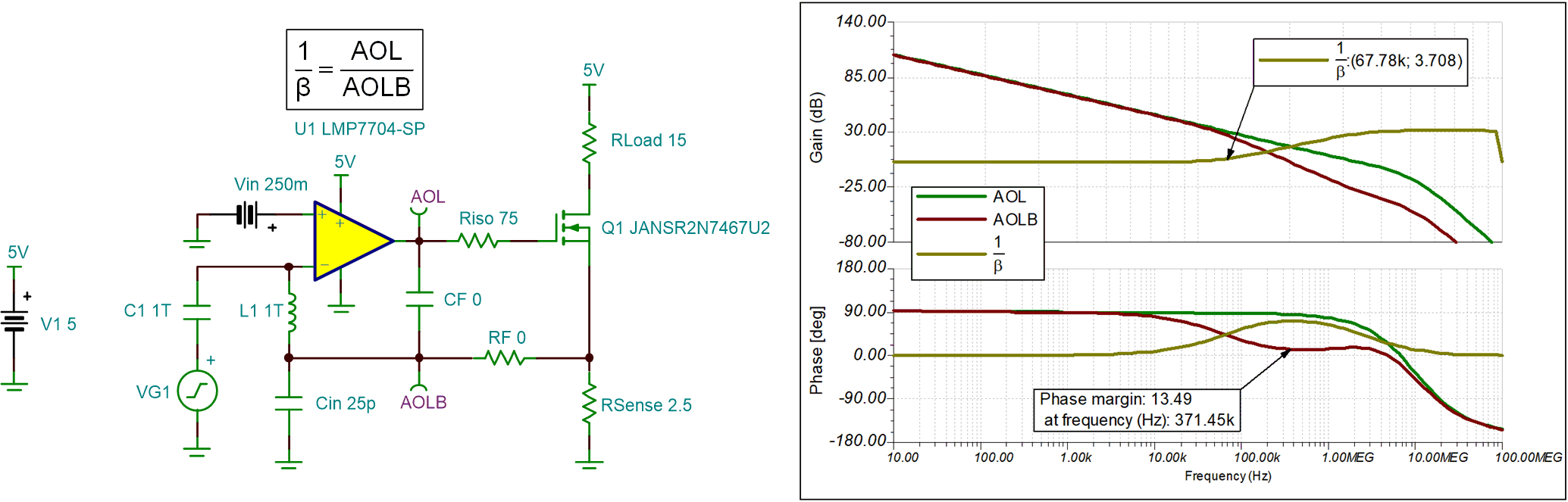
- The simple fix to this is
to create a high frequency pole in 1/β and bypass the MOSFET at higher
frequencies. By adding the capacitor CF, the amplifier returns to unity
gain over the frequency range of interest. Calculate the value of CF by
looking at the location of the 1/β zero (fz1/β), shown in the
previous figure as 67.78kHz. The value of CF is then calculated as:
- With CF added, the new
open loop AC response looks like the following:

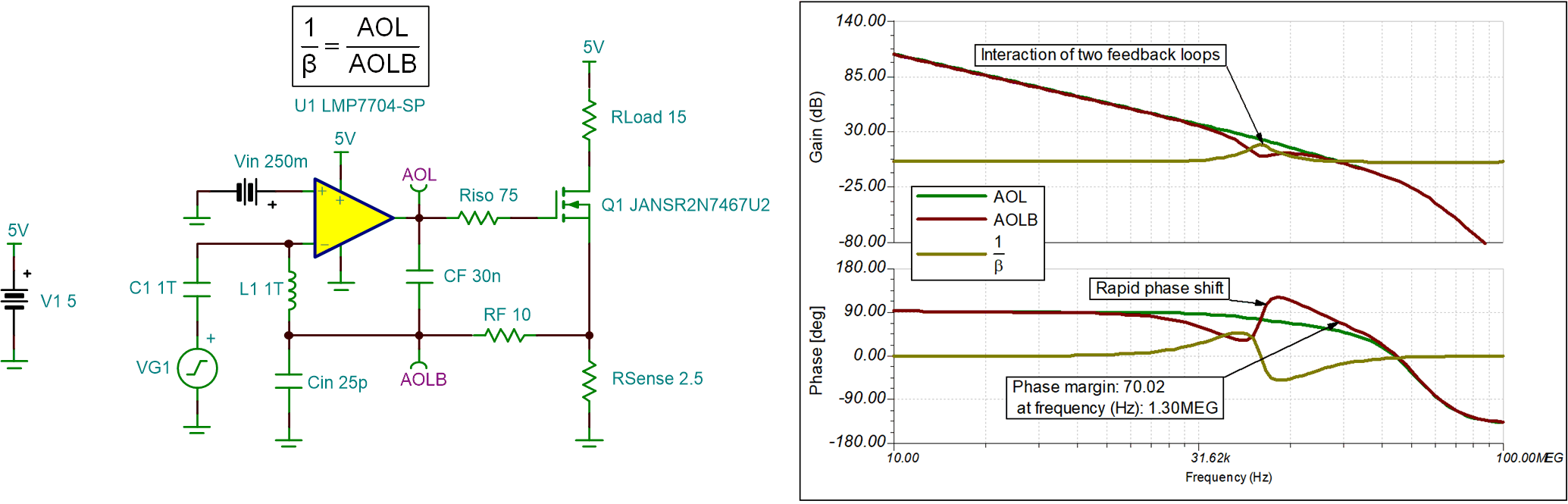
- CF successfully formed
the pole in 1/β; however, there is peaking in 1/β that causes
instability. This occurs when CF interacts with the transconductance of
the MOSFET. The effect of the interaction is two feedback loops to the
amplifier. In this case, both feedback loops interact with each other
around the resonant frequency. Adding a small value for RF (10Ω) can
isolate the two feedback loops. With an RF of 10Ω, the circuit seems to
have 70° of phase margin at fcl; however, in reality, it is still not
stable. The next figure shows the instability through the rapid phase
shifts in AOLB and the peaking in 1/β.
- This may be confirmed by
looking at the small signal transient step response which shows
oscillation at the resonant frequency of about 170kHz for small values
of RF.
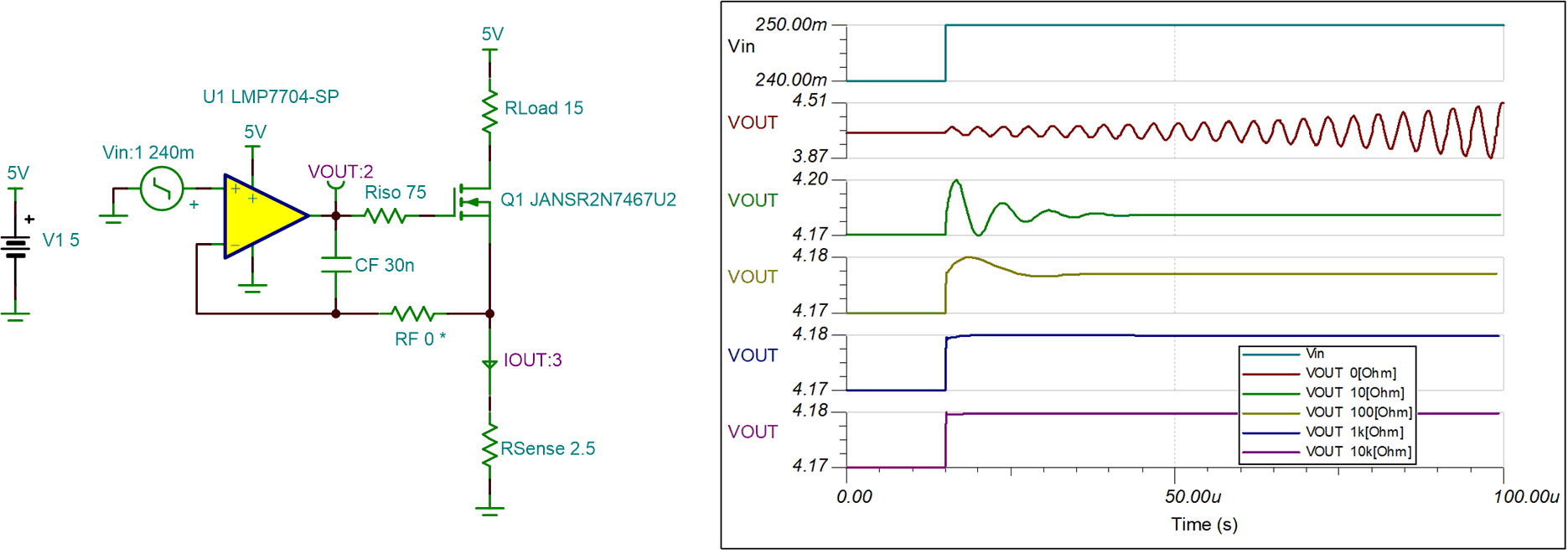
- The final step to stabilizing the circuit is to add a sufficiently large resistor (RF) to flatten out 1/β and fully isolate CF from the MOSFET. Obtain the final value of RF through trial-and-error until the desired small signal step response is achieved. Typically, RF is in the range of 1kΩ to 10kΩ. The final open loop AC response is seen in the AC Simulation Results section. As seen from the previous simulation, different RF values yield different small signal step responses. With a zero or small RF value, oscillations and overshoot is observed. A value of 1kΩ for RF is sufficient to give the desired small signal transient response.