SPRACL9 May   2019 66AK2E05 , 66AK2H06 , 66AK2H12 , 66AK2H14 , AM5K2E02 , AM5K2E04 , TMS320C6652 , TMS320C6654 , TMS320C6655 , TMS320C6657 , TMS320C6670 , TMS320C6671 , TMS320C6672 , TMS320C6674 , TMS320C6678


  1.   KeyStone Multicore Device Family Schematic Checklist
    1.     Trademarks
    2. 1 Introduction
    3. 2 Hardware Design Guide
    4. 3 Device Comparison
      1. 3.1 KeyStone II Devices
      2. 3.2 KeyStone I Devices
    5. 4 Power Management Solutions
    6. 5 Recommendations Specific to all KeyStone Devices
      1. 5.1 EVM vs Data Sheet
      2. 5.2 Critical Connections
        1. 5.2.1 Power
        2. 5.2.2 Clocking
        3. 5.2.3 LJCB Differential Clock Inputs
        4. 5.2.4 Clock Termination
        5. 5.2.5 Unused Clock Inputs
        6. 5.2.6 Reset
        7. 5.2.7 GPIO/Boot Configuration
        8. 5.2.8 JTAG and EMU
    7. 6 Peripherals
      1. 6.1 DDR3 Interface
        1. 6.1.1  EMIF16
        2. 6.1.2  SerDes
        3. 6.1.3  HyperLink
        4. 6.1.4  PCIe
        5. 6.1.5  SRIO
        6. 6.1.6  SGMII
        7. 6.1.7  MDIO
        8. 6.1.8  TSIP
        9. 6.1.9  I2C
        10. 6.1.10 SPI
        11. 6.1.11 UART
        12. 6.1.12 I/O Buffers and Termination
    8. 7 Recommendations Specific to KeyStone II Devices
      1. 7.1 Peripherals
        1. 7.1.1 USB
    9. 8 General Recommendations
      1. 8.1 Before You Begin
        1. 8.1.1 Documentation
        2. 8.1.2 Pinout
    10. 9 References

Unused Clock Inputs

Any unused LJCB or LVDS differential clock inputs should be connected to the appropriate rails to establish a valid logic level. Unused clock inputs connected to the SerDes/CML in the KeyStone II device should be left unconnected. The recommended connections are shown in Figure 3 and Figure 4. The added 1kΩ resistor is designed to reduce power consumption. The positive terminal should be connected to the respective power rail. For more clarity, see Hardware Design Guide for KeyStone™ I Devices and the Hardware Design Guide for KeyStone II Devices.
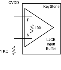
spracl9-unused-ljcb-clock-input-connection.gifFigure 3. Unused LJCB Clock Input Connection
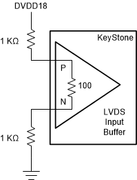
spracl9-unused-lvds-clock-input-connection.gifFigure 4. Unused LVDS Clock Input Connection