SPRUJ40C may 2022 – may 2023
- 1
- Abstract
- Trademarks
- 1EVM Revisions and Assembly Variants
-
2System Description
- 2.1 Key Features
- 2.2 Functional Block Diagram (SK-AM62 and SK-AM62B)
- 2.3 Functional Block Diagram (SK-AM62-P1 and SK-AM62B-P1)
- 2.4 AM62x SKEVM Interface Mapping
- 2.5 Power ON/OFF Procedures
- 2.6
Peripheral and Major Component
Description
- 2.6.1 Clocking
- 2.6.2 Reset
- 2.6.3 OLDI Display Interface
- 2.6.4 CSI Interface
- 2.6.5 Audio Codec Interface
- 2.6.6 HDMI Display Interface
- 2.6.7 JTAG Interface
- 2.6.8 Test Automation Header
- 2.6.9 UART Interface
- 2.6.10 USB Interface
- 2.6.11 Memory Interfaces
- 2.6.12 Ethernet Interface
- 2.6.13 GPIO Port Expander
- 2.6.14 GPIO Mapping
- 2.6.15 Power
- 2.6.16 AM62x SKEVM User Setup/Configuration
- 2.6.17 Expansion Headers
- 2.6.18 Interrupt
- 2.6.19 I2C Address Mapping
-
3Known Issues and Modifications
- 3.1 Issue 1 - HDMI/DSS Incorrect Colors on E1
- 3.2 Issue 2 - J9 and J10 Header Alignment on E1
- 3.3 Issue 3 - USB Boot descoped on E1
- 3.4 Issue 4 - OLDI Connector Orientation and Pinout
- 3.5 Issue 5 - Bluetooth descoped on E2 EVMs
- 3.6 Issue 6 - Ethernet PHY CLK Skew Default Strapping Changes
- 3.7 Issue 7 - TEST_POWERDOWN changes
- 3.8 Issue 8 - MMC1_SDCD spurious interrupts
- 3.9 Issue 9 - PD Controller I2C2 IRQ Not Pinned Out
- 3.10 Issue 10 - INA Current Monitor Adress Changes
- 3.11 Issue 11 - Test Automation I2C Buffer Changes
- Regulatory Compliance
- Revision History
2.6.5 Audio Codec Interface
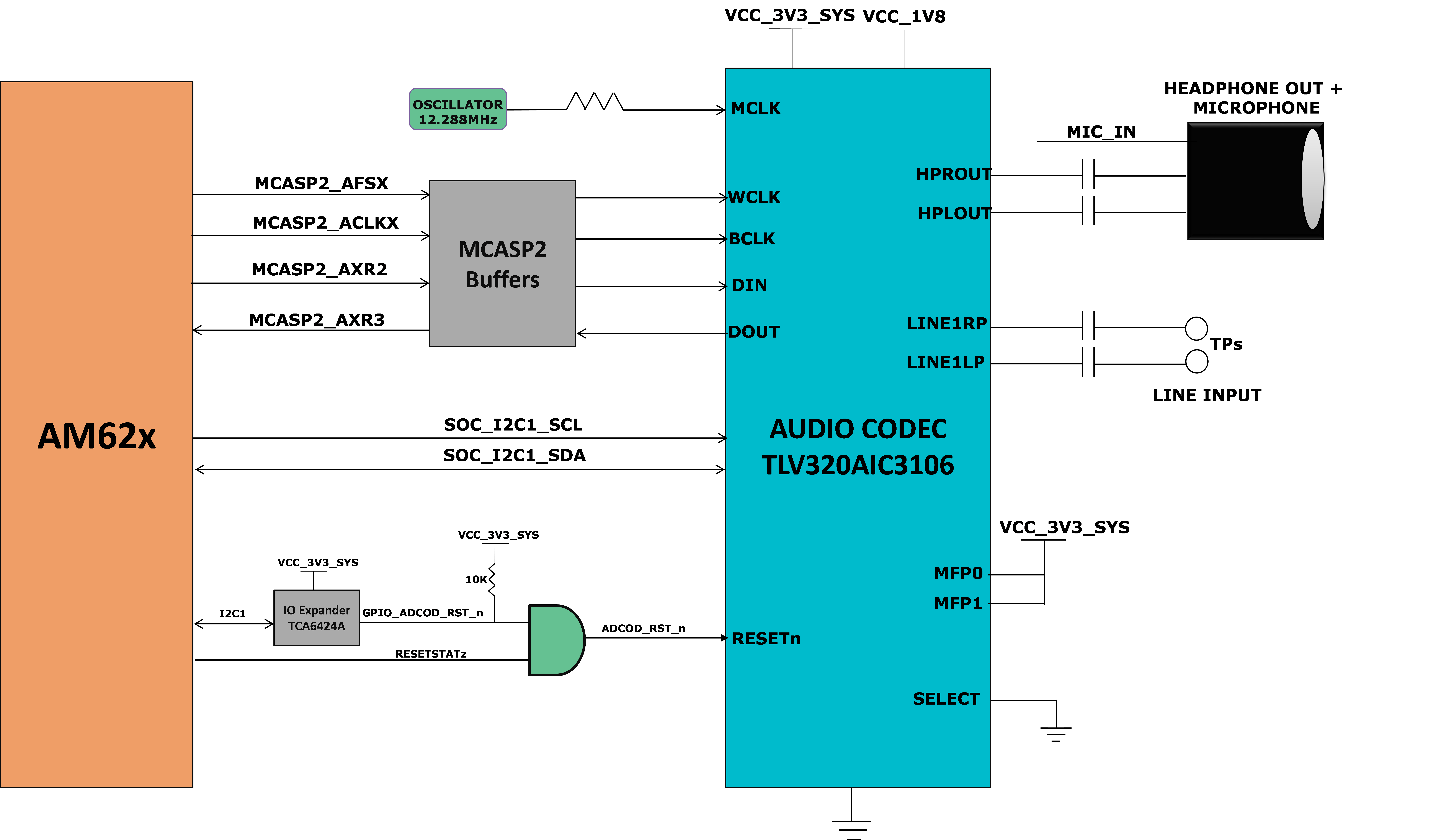
AM62x SKEVM has TI‘s Low-Power TLV320AIC3106 Stereo Audio Codec to interface with AM62x via McASP.
TLV320AIC3106 is a low-power stereo audio codec with stereo headphone amplifier, as well as multiple inputs and outputs programmable in single ended or fully differential configurations. The record path of the TLV320AIC3106 contains integrated microphone bias, digitally controlled stereo microphone preamplifier and automatic gain control (AGC) with mix/Mux capability among the multiple analog inputs. The stereo audio DAC supports sampling rates from 8 kHz to 96 kHz.
1x Standard 3.5 mm TRRS Audio Jack connector Mfr. Part# SJ-43514 shall be provided for MIC and Headphone output. Audio Codec’s Line inputs are terminated to Testpoints.
SELECT pin shall be held LOW to select I2C as control interface. Codec can be configured over I2C interface, where I2C address can be set by driving pins MFP0 and MFP1 pin either high or low. Both these pins are set to high, so the Device address is set to 0x1B. Unused inputs and outputs of the Audio Codec are connected to ground.
The Controller Clock input, MCLK to the Audio Codec is provided through a 12.288MHz Oscillator. Audio serial data bus bit clock BCLK of \the codec is driven by the AM62x SoC through a buffer. Audio serial data bus input and output DIN, DOUT are connected to SoC’s MCASP2_AXR2 and MCASP2_AXR3 through buffers. An AND output of RESETSTATz and a GPIO sourced via IO expander are used to reset the Audio codec.
The TLV320AIC3106 is powred by an analog supply of 3.3 V, a digital core supply of 1.8 V, and a digital I/O supply 3.3 V.
