SPRUJ40C may 2022 – may 2023
- 1
- Abstract
- Trademarks
- 1EVM Revisions and Assembly Variants
-
2System Description
- 2.1 Key Features
- 2.2 Functional Block Diagram (SK-AM62 and SK-AM62B)
- 2.3 Functional Block Diagram (SK-AM62-P1 and SK-AM62B-P1)
- 2.4 AM62x SKEVM Interface Mapping
- 2.5 Power ON/OFF Procedures
- 2.6
Peripheral and Major Component
Description
- 2.6.1 Clocking
- 2.6.2 Reset
- 2.6.3 OLDI Display Interface
- 2.6.4 CSI Interface
- 2.6.5 Audio Codec Interface
- 2.6.6 HDMI Display Interface
- 2.6.7 JTAG Interface
- 2.6.8 Test Automation Header
- 2.6.9 UART Interface
- 2.6.10 USB Interface
- 2.6.11 Memory Interfaces
- 2.6.12 Ethernet Interface
- 2.6.13 GPIO Port Expander
- 2.6.14 GPIO Mapping
- 2.6.15 Power
- 2.6.16 AM62x SKEVM User Setup/Configuration
- 2.6.17 Expansion Headers
- 2.6.18 Interrupt
- 2.6.19 I2C Address Mapping
-
3Known Issues and Modifications
- 3.1 Issue 1 - HDMI/DSS Incorrect Colors on E1
- 3.2 Issue 2 - J9 and J10 Header Alignment on E1
- 3.3 Issue 3 - USB Boot descoped on E1
- 3.4 Issue 4 - OLDI Connector Orientation and Pinout
- 3.5 Issue 5 - Bluetooth descoped on E2 EVMs
- 3.6 Issue 6 - Ethernet PHY CLK Skew Default Strapping Changes
- 3.7 Issue 7 - TEST_POWERDOWN changes
- 3.8 Issue 8 - MMC1_SDCD spurious interrupts
- 3.9 Issue 9 - PD Controller I2C2 IRQ Not Pinned Out
- 3.10 Issue 10 - INA Current Monitor Adress Changes
- 3.11 Issue 11 - Test Automation I2C Buffer Changes
- Regulatory Compliance
- Revision History
2.6.4 CSI Interface
The CSI-2 interface from the AM62x SoC is terminated to a 15 pin Camera FPC connector 1-1734248-5 compatible with the RPi Camera Modules. These modules support 2 Lane CSI RX signals. While the SoC supports 4 CSI RX Lanes, only two are pinned out on the SKEVM
The CSI connector pin-out is compatible with the RPi camera connector. The Table 2-6 contains 15 pin CSI Connector pin-out. SoC I2C1 signals are also connected to the CSI Header. IO Expander GPIO signals are connected to the camera GPIO’s.
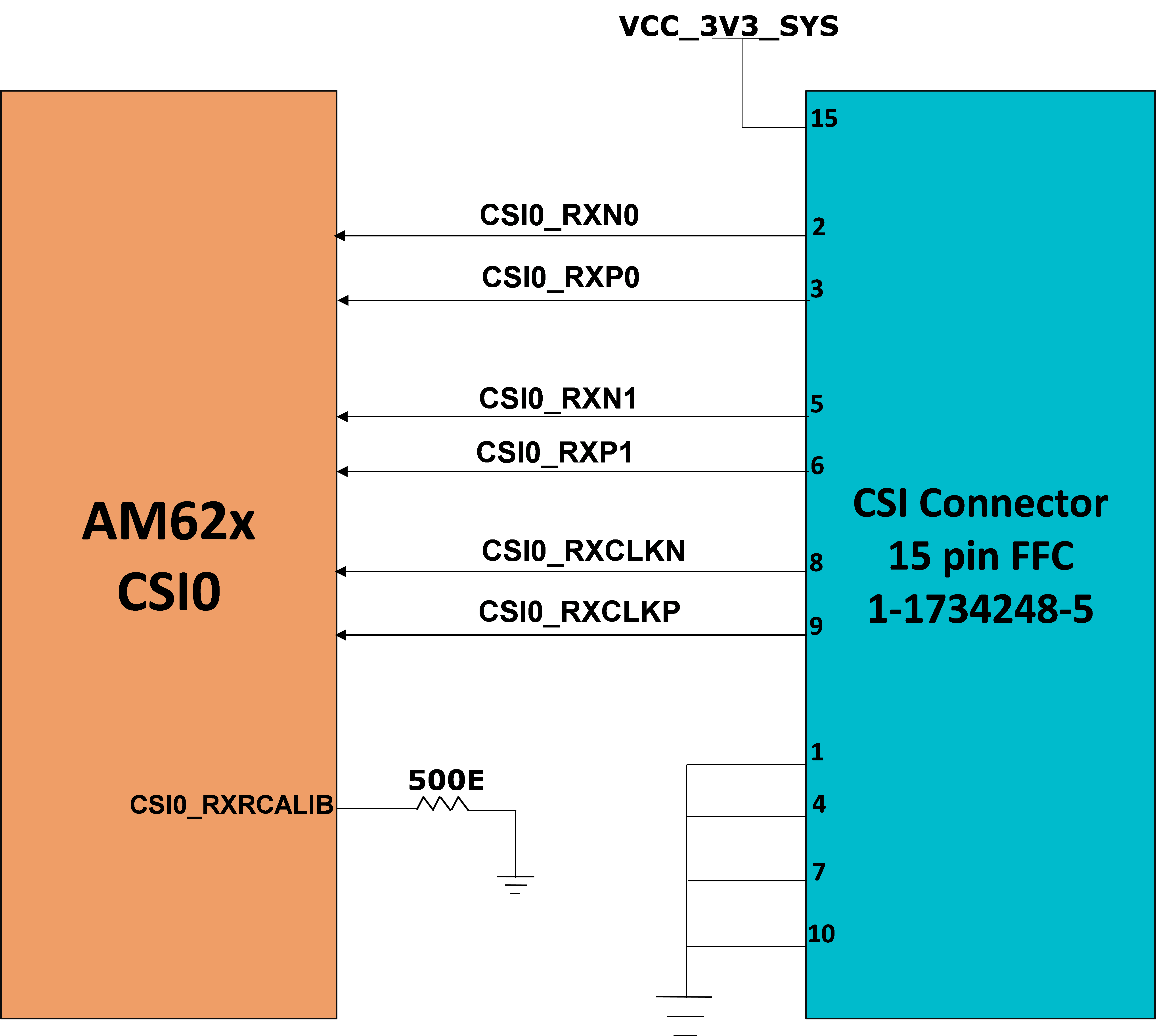
Table 2-6 CSI Camera Connector J19
Pin-out
| Pin No | Pin Description |
|---|---|
| 1 | Ground |
| 2 | CSI0_RXN0 |
| 3 | CSI0_RXP0 |
| 4 | Ground |
| 5 | CSI0_RXN1 |
| 6 | CSI0_RXP1 |
| 7 | Ground |
| 8 | CSI0_RXCLKN |
| 9 | CSI0_RXCLKP |
| 10 | Ground |
| 11 | CSI_GPIO1 |
| 12 | CSI_GPIO2 |
| 13 | SoC_I2C1_SCL |
| 14 | SoC_I2C1_SDA |
| 15 | VCC_3V3_SYS |