SWRU585 November 2021 IWR6843
- Trademarks
- 1Getting Started
- 2Hardware
- 3PCB Storage and Handling Recommendations
- 4IWR6843LEVM Antenna
-
5Hardware Details
- 5.1 Switch Settings
- 5.2 LEDs
- 5.3 Connectors
- 5.4 USB Connector
- 5.5 DCA1000 HD Connector
- 5.6 MMWAVEICBOOST HD Connector
- 5.7 CANFD Connector
- 5.8 I2C Connections
- 5.9 EEPROM
- 5.10 Default I2C Address
- 5.11 Modular Mode
- 5.12 Flashing the Board
- 5.13 DCA1000EVM Mode
- 5.14 MMWAVEICBOOST Mode
- 5.15 Raw ADC Data Capture Using MMWAVEICBOOST and DCA1000 EVMs
- 5.16 Muxing Scheme
- 6Software, Development Tools, and Example Code
- 7TI E2E Community
- 8References
5.7 CANFD Connector
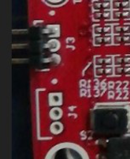
The CAN connector provides access to the two CAN_FD interfaces (CAN_L and CAN_H signals) from the onboard CAND-FD transceivers. These signals can be directly wired to the CAN bus.
 Figure 5-5 CANFD Connector
Table 5-3 shows the J3 and J4 connectors that provide the CAN_L and CAN_H signals from the 2 onboard CAND-FD transceivers (TCAN1042HGVDRQ1). These signals are wired to the CAN bus after muxing with the SPI interface signals; one of the two paths must be selected. Two CANs are selected by closing the switch S1.4 (1st position of switch to be ON).
Table 5-3 CAN Pin Assignment
| Pin Description | Device Interface | Connector on Board |
|---|---|---|
| SPI_CS1 | CAN2_TX | J4.1 - CANL, J4.2 - GND, J4.3 - CANH |
| SPI_CLK1 | CAN2_RX | |
| MISO_1 | CAN1_TX | J3.1 - CANL, J3.2 - GND, J3.3 - CANH |
| MOSI_1 | CAN1_RX |