TIDT224 March   2021


  1. 1Description
  2. 2Test Prerequisites
    1. 2.1 Voltage and Current Requirements
    2. 2.2 Required Equipment
  3. 3Testing and Results
    1. 3.1 Thermal Images
    2. 3.2 Efficiency and Power Dissipation Graphs
    3. 3.3 Efficiency and Power Dissipation Data
    4. 3.4 Voltage Regulation Graphs
    5. 3.5 Cross-Load Voltage Regulation Data and Efficiency
  4. 4Waveforms
    1. 4.1 Start-up Sequence
    2. 4.2 Switch Node
    3. 4.3 Output Voltage Ripple
    4. 4.4 Load Transients

Load Transients

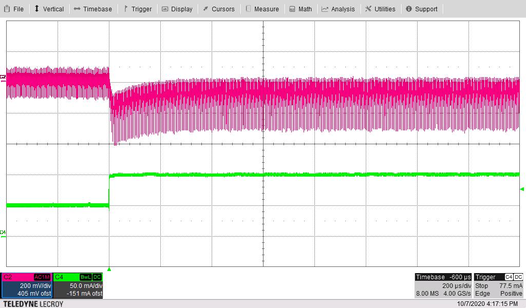
The following image shows the 15-V output voltage (AC coupled, Red) when the load current (Green) is stepped from 50 mA to 100 mA. The second output is loaded to 100 mA and the input voltage is 12 VDC.
GUID-20210223-CA0I-GP8Z-PBDZ-RRTBSV4HZFP1-low.jpg
200 mV/div, 50 mA/div, 200 µs/div
Figure 4-14 Load Transients, 15-V Output Voltage

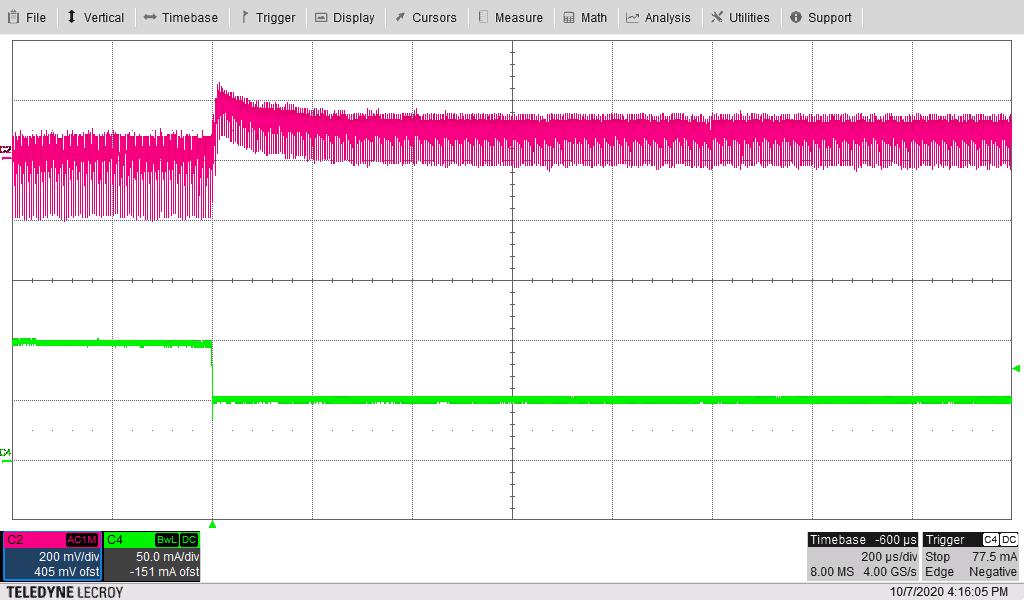
The following image shows the 15-V output voltage (AC coupled, Red) when the load current (Green) is stepped from 100 mA to 50 mA. The second output is loaded to 100 mA and the input voltage is 12 VDC.
GUID-20210223-CA0I-50ZJ-R1LH-GJWDMS8TNTBN-low.jpg
200 mV/div, 50 mA/div, 200 µs/div
Figure 4-15 Load Transients, 15-V Output Voltage

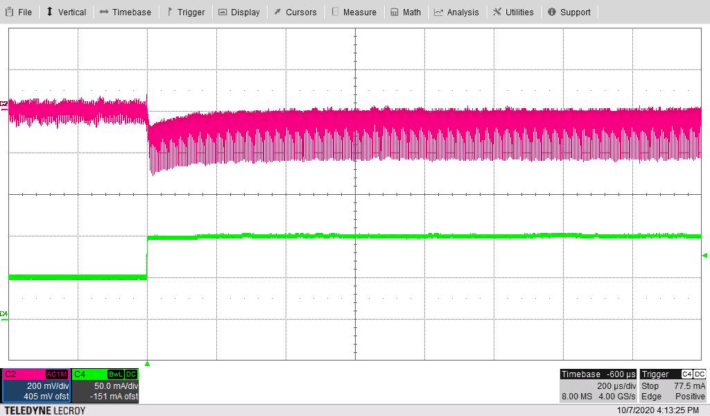
The following image shows the 15-V output voltage (AC coupled, Red) when the load current (Green) is stepped from 50 mA to 100 mA. The second output is loaded to 100 mA and the input voltage is 15 VDC.
GUID-20210223-CA0I-V7SM-MRWK-M24HRD7F7PXB-low.jpg
200 mV/div, 50 mA/div, 200 µs/div
Figure 4-16 Load Transients, 15-V Output Voltage

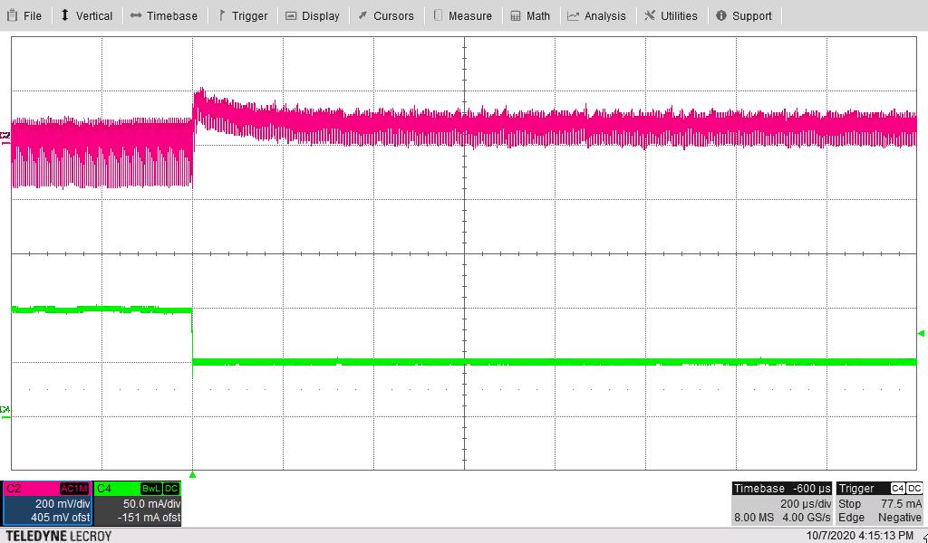
The following image shows the 15-V output voltage (AC coupled, Red) when the load current (Green) is stepped from 100 mA to 50 mA. The second output is loaded to 100 mA and the input voltage is 15 VDC.
GUID-20210223-CA0I-PF0W-G1TJ-P0PRGMGVXZHZ-low.jpg
200 mV/div, 50 mA/div, 200 µs/div
Figure 4-17 Load Transients, 15-V Output Voltage