TIDT224 March   2021


  1. 1Description
  2. 2Test Prerequisites
    1. 2.1 Voltage and Current Requirements
    2. 2.2 Required Equipment
  3. 3Testing and Results
    1. 3.1 Thermal Images
    2. 3.2 Efficiency and Power Dissipation Graphs
    3. 3.3 Efficiency and Power Dissipation Data
    4. 3.4 Voltage Regulation Graphs
    5. 3.5 Cross-Load Voltage Regulation Data and Efficiency
  4. 4Waveforms
    1. 4.1 Start-up Sequence
    2. 4.2 Switch Node
    3. 4.3 Output Voltage Ripple
    4. 4.4 Load Transients

Switch Node

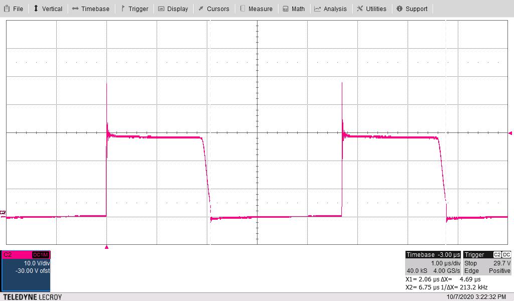
The following image shows the FET switch node voltage SW (Red) at TP4. The input voltage is 12 VDC and both 15-V outputs are loaded to 100 mA.
GUID-20210223-CA0I-NTGJ-MP2L-77TW3CCRB7SD-low.jpg
10 V/div, 1 µs/div
Figure 4-4 FET Switch Node Voltage SW

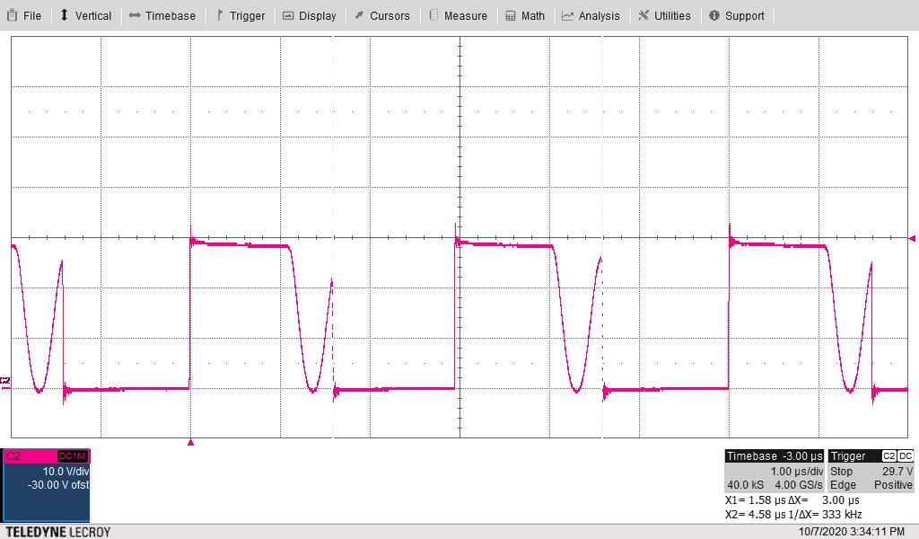
The following image shows the FET switch node voltage SW (Red) at TP4. The input voltage is 12 VDC and both 15-V outputs are loaded to 50 mA.
GUID-20210223-CA0I-KT0G-VKFB-5W501P4HRVH8-low.jpg
10 V/div, 1 µs/div
Figure 4-5 FET Switch Node Voltage SW

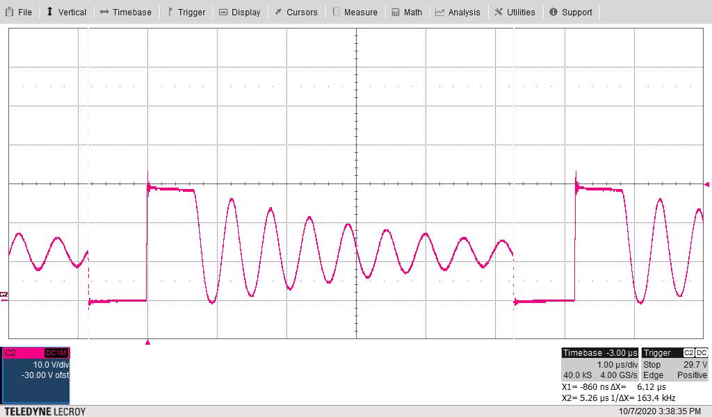
The following image shows the FET switch node voltage SW (Red) at TP4. The input voltage is 12 VDC and both 15-V outputs are loaded to 10 mA.
GUID-20210223-CA0I-WMHG-GHGZ-2CM7MNW46PDQ-low.jpg
10 V/div, 1 µs/div
Figure 4-6 FET Switch Node Voltage SW

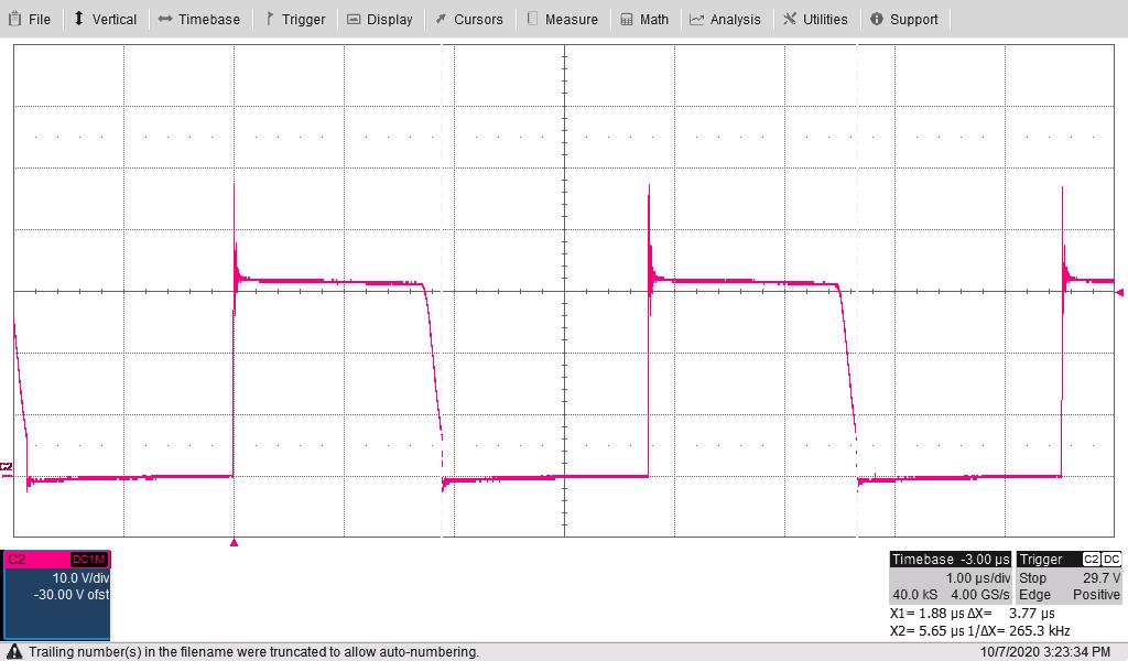
The following image shows the FET switch node voltage SW (Red) at TP4. The input voltage is 15 VDC and both 15-V outputs are loaded to 100 mA.
GUID-20210223-CA0I-BJP8-PKBJ-WQZDJWSMSNBW-low.jpg
10 V/div, 1 µs/div
Figure 4-7 FET Switch Node Voltage SW

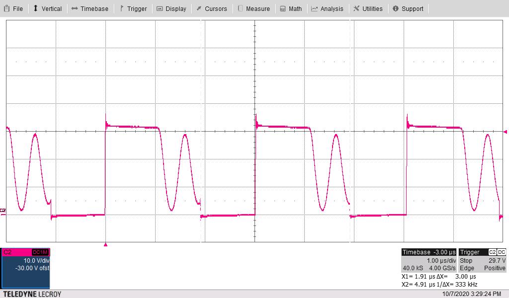
The following image shows the FET switch node voltage SW (Red) at TP4. The input voltage is 15 VDC and both 15-V outputs are loaded to 50 mA.
GUID-20210223-CA0I-SMJJ-485R-50JSZWW5NQZS-low.jpg
10 V/div, 1 µs/div
Figure 4-8 FET Switch Node Voltage SW

The following image shows the FET switch node voltage SW (Red) at TP4. The input voltage is 15 VDC and both 15-V outputs are loaded to 10 mA.

GUID-20210223-CA0I-W8DL-MFWK-6427QN6VZ8HJ-low.jpg
10 V/div, 1 µs/div
Figure 4-9 FET Switch Node Voltage SW

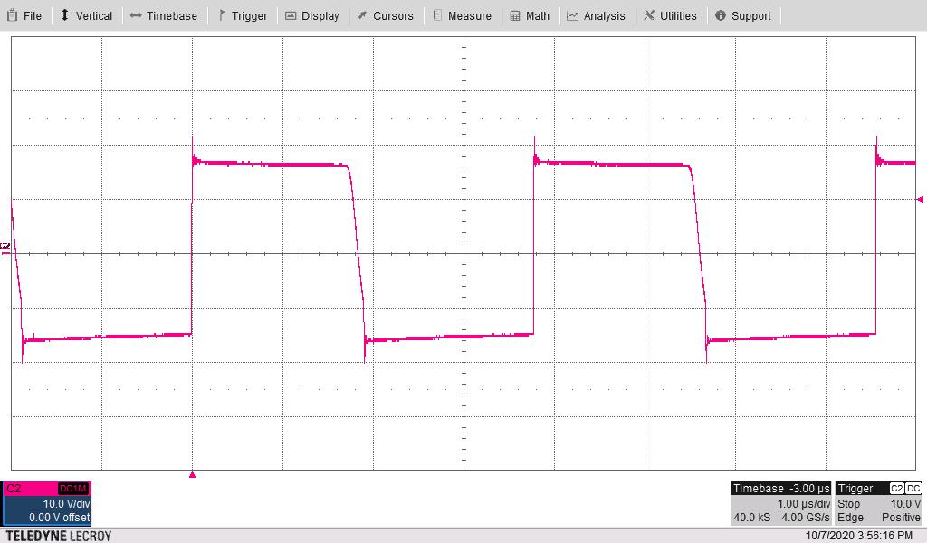
The following image shows the secondary winding voltage of the transformer at T1- pin 5 (Red) with respect to T1 – pin 6. The input voltage is 15 VDC and both 15-V outputs are loaded to 100 mA.
GUID-20210223-CA0I-XHTH-HD77-TJJ6SSBBFBGR-low.jpg
10 V/div, 1 µs/div
Figure 4-10 Secondary Winding Voltage of the Transformer

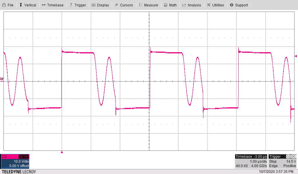
The following image shows the secondary winding voltage of the transformer at T1- pin 5 (Red) with respect to T1 – pin 6. The input voltage is 15 VDC and both 15-V outputs are loaded to 50 mA.
GUID-20210223-CA0I-9LSJ-WVQD-5HKQFPGKXSJ0-low.jpg
10 V/div, 1 µs/div
Figure 4-11 Secondary Winding Voltage of the Transformer