TIDT244 July 2021
3.2 Efficiency and Power Dissipation Graph
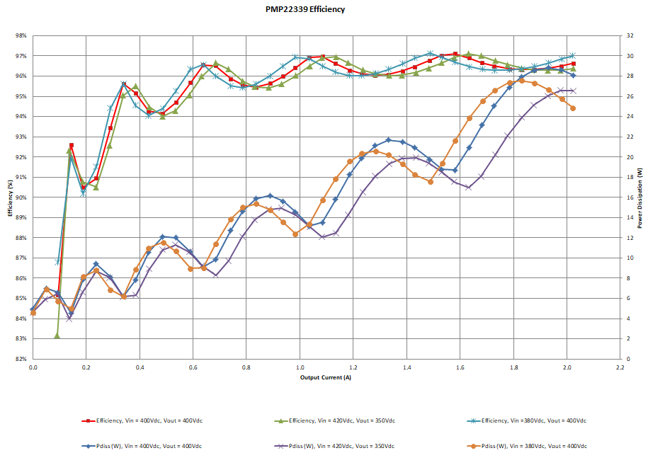
This graph displays the efficiency and power dissipation of the converter at three different input and output voltage conditions.
 Figure 3-3 Efficiency and Power Dissipation Graph
TIDT244 July 2021
This graph displays the efficiency and power dissipation of the converter at three different input and output voltage conditions.
 Figure 3-3 Efficiency and Power Dissipation Graph