TIDT244 July   2021


  1. 1Description
  2. 2Test Prerequisites
    1. 2.1 Voltage and Current Requirements
    2. 2.2 Required Equipment
  3. 3Testing and Results
    1. 3.1 Thermal Images
    2. 3.2 Efficiency and Power Dissipation Graph
    3. 3.3 Efficiency and Power Dissipation Data
    4. 3.4 Current Regulation
    5. 3.5 Voltage Regulation
  4. 4Waveforms
    1. 4.1 Start-up
    2. 4.2 Switch Node
    3. 4.3 Output Voltage Ripple
    4. 4.4 Current Loop to Voltage Loop Transition
    5. 4.5 Voltage Loop to Current Loop Transition
    6. 4.6 Bias Voltage Start-up
    7. 4.7 Bias Voltage Switch Nodes
    8. 4.8 Output Current Sense Signal

Output Voltage Ripple

The output ripple voltage is shown in the following figure. The ripple was measured tip and barrel across ceramic output capacitors C10 and C14.
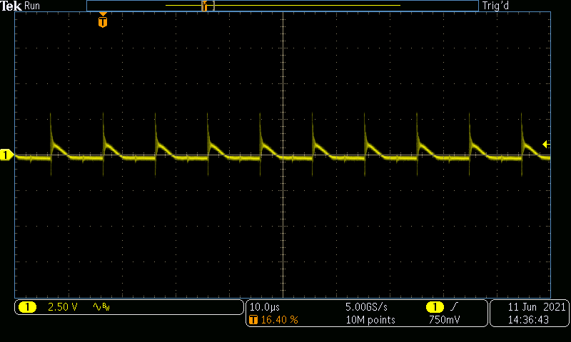
GUID-20210611-CA0I-DJB9-3DKB-HCZKZN5QV01S-low.pngFigure 4-9 VIN = 400 V and VOUT = 400 V at 2 A. Resistive Load (VOUT: 2.5 V/DIV, 10 µs/DIV, BWL = 20 MHz)