TIDT244 July   2021


  1. 1Description
  2. 2Test Prerequisites
    1. 2.1 Voltage and Current Requirements
    2. 2.2 Required Equipment
  3. 3Testing and Results
    1. 3.1 Thermal Images
    2. 3.2 Efficiency and Power Dissipation Graph
    3. 3.3 Efficiency and Power Dissipation Data
    4. 3.4 Current Regulation
    5. 3.5 Voltage Regulation
  4. 4Waveforms
    1. 4.1 Start-up
    2. 4.2 Switch Node
    3. 4.3 Output Voltage Ripple
    4. 4.4 Current Loop to Voltage Loop Transition
    5. 4.5 Voltage Loop to Current Loop Transition
    6. 4.6 Bias Voltage Start-up
    7. 4.7 Bias Voltage Switch Nodes
    8. 4.8 Output Current Sense Signal

Voltage Regulation

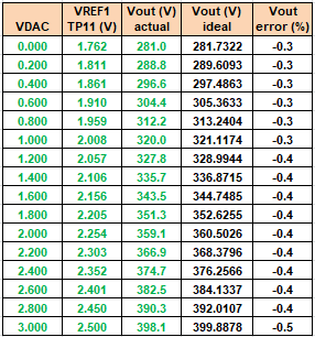
This graph displays the measured output voltage versus CHG VSET DAC at an input voltage of 400 Vdc. A DC voltage ranging from 0 V–3 V is applied at J6 and a constant resistance mode load is used with the resistance equal to VOUT ideal at each setpoint.
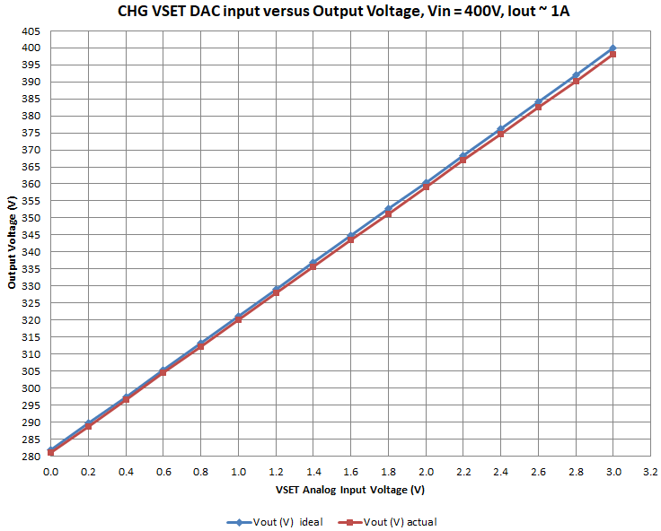
GUID-20210611-CA0I-PBHQ-XTCR-1JKJCDZT9NVN-low.pngFigure 3-9 CHG VSET DAC Accuracy Curve
GUID-20210614-CA0I-FKM1-D8PM-DJBJHDMG6HJB-low.pngFigure 3-10 CHG VSET DAC Accuracy Table