TIDT244 July 2021
4.8 Output Current Sense Signal
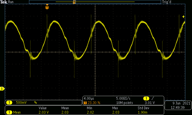
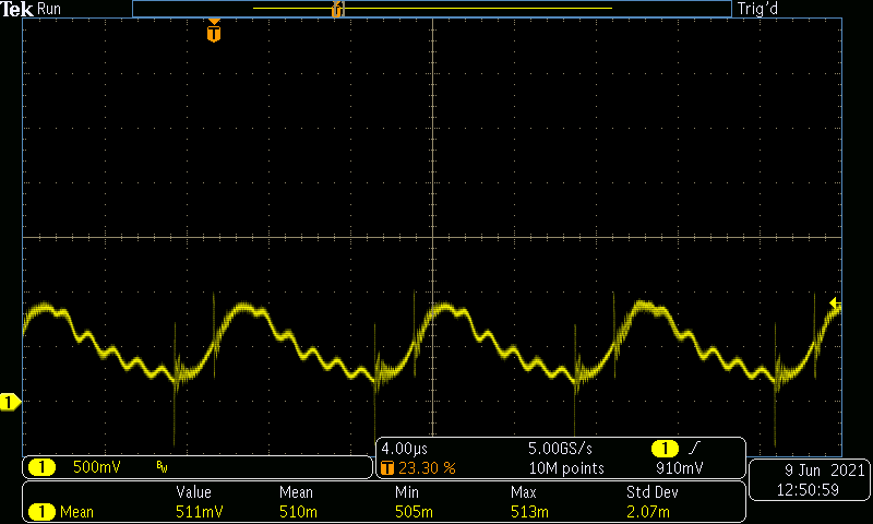
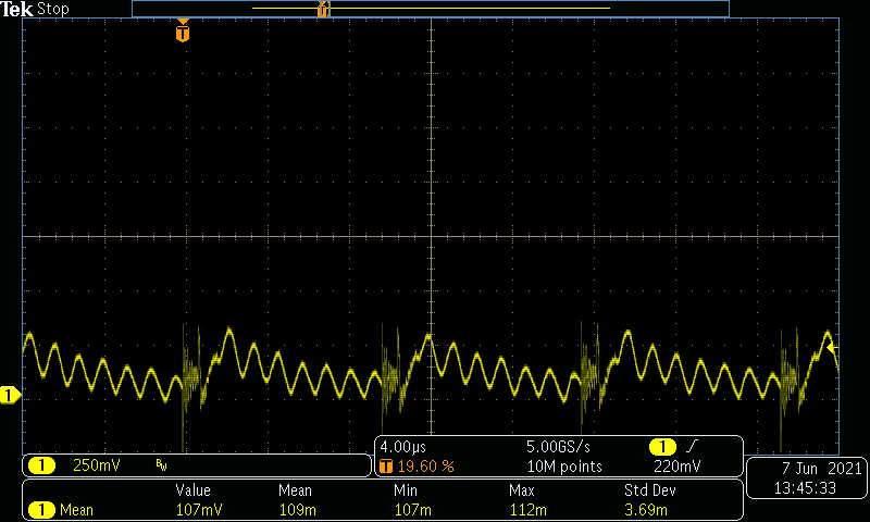
The average of the MB CHG ISNS signal (on TP1) can be used to monitor the output current of the power supply. The following figures show the signal shape for varying output conditions.
 Figure 4-15 VIN = 400 V, VOUT = 400
V, IOUT = 2 A.
Figure 4-15 VIN = 400 V, VOUT = 400
V, IOUT = 2 A.I_mean = 2.03 V (500 mV/DIV, 4 µs/DIV, BWL = 20 MHz)
 Figure 4-16 VIN = 400 V, VOUT = 400
V, IOUT = 500 mA.
Figure 4-16 VIN = 400 V, VOUT = 400
V, IOUT = 500 mA.I_mean = 511 mV (500 mV/DIV, 4 µs/DIV, BWL = 20 MHz)
 Figure 4-17 VIN = 400 V, VOUT = 400
V, IOUT = 100 mA.
Figure 4-17 VIN = 400 V, VOUT = 400
V, IOUT = 100 mA.I_mean = 107 mV (500 mV/DIV, 4 µs/DIV, BWL = 20 MHz)