TIDT244 July   2021


  1. 1Description
  2. 2Test Prerequisites
    1. 2.1 Voltage and Current Requirements
    2. 2.2 Required Equipment
  3. 3Testing and Results
    1. 3.1 Thermal Images
    2. 3.2 Efficiency and Power Dissipation Graph
    3. 3.3 Efficiency and Power Dissipation Data
    4. 3.4 Current Regulation
    5. 3.5 Voltage Regulation
  4. 4Waveforms
    1. 4.1 Start-up
    2. 4.2 Switch Node
    3. 4.3 Output Voltage Ripple
    4. 4.4 Current Loop to Voltage Loop Transition
    5. 4.5 Voltage Loop to Current Loop Transition
    6. 4.6 Bias Voltage Start-up
    7. 4.7 Bias Voltage Switch Nodes
    8. 4.8 Output Current Sense Signal

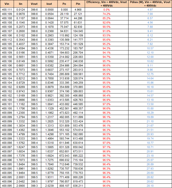
Efficiency and Power Dissipation Data

GUID-20210614-CA0I-G6FV-4JLF-2XWHRCLND6VL-low.png Figure 3-4 Efficiency and Power Dissipation at VIN = 400 Vdc, VOUT = 400 Vdc
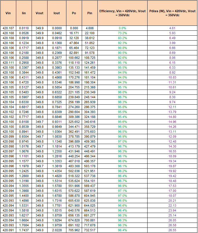
GUID-20210614-CA0I-GMG5-PR5V-ZKJCVXSPXWBC-low.png Figure 3-5 Efficiency and Power Dissipation at VIN = 420 Vdc, VOUT = 350 Vdc
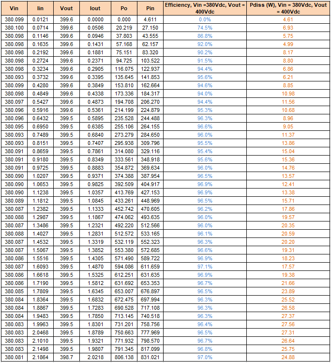
GUID-20210616-CA0I-K720-F742-KNNCMBJS0FZX-low.png Figure 3-6 Efficiency and Power Dissipation at VIN = 380 Vdc, VOUT = 400 Vdc