TIDT244 July 2021
4.2 Switch Node
The following figures show the FET switch node voltage (YELLOW) at TP7 under various input and output conditions.
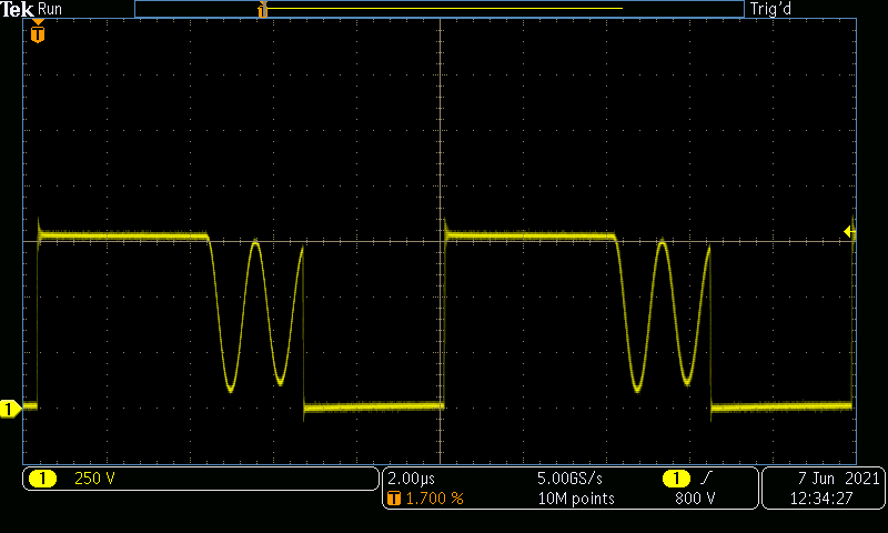 Figure 4-3 VIN = 420 V and VOUT =
350 V at 2 A.
Figure 4-3 VIN = 420 V and VOUT =
350 V at 2 A.Resistive Load (VOUT: 250 V/DIV, 2 µs/DIV, BWL = 800 MHz)
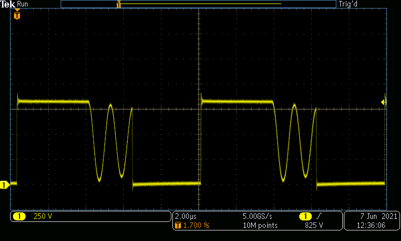 Figure 4-4 VIN = 420 V and VOUT =
400 V at 2 A.
Figure 4-4 VIN = 420 V and VOUT =
400 V at 2 A.Resistive Load (VOUT: 250 V/DIV, 2 µs/DIV, BWL = 800 MHz)
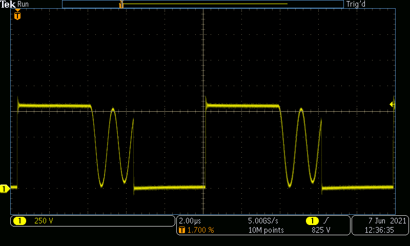 Figure 4-5 VIN = 400 V and VOUT =
400 V at 2 A.
Figure 4-5 VIN = 400 V and VOUT =
400 V at 2 A.Resistive Load (VOUT: 250 V/DIV, 2 µs/DIV, BWL = 800 MHz)
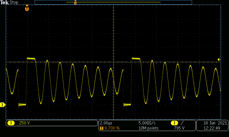 Figure 4-6 VIN = 400 V and VOUT =
400 V at 70 mA.
Figure 4-6 VIN = 400 V and VOUT =
400 V at 70 mA.Resistive Load (VOUT: 250 V/DIV, 2 µs/DIV, BWL = 800 MHz)
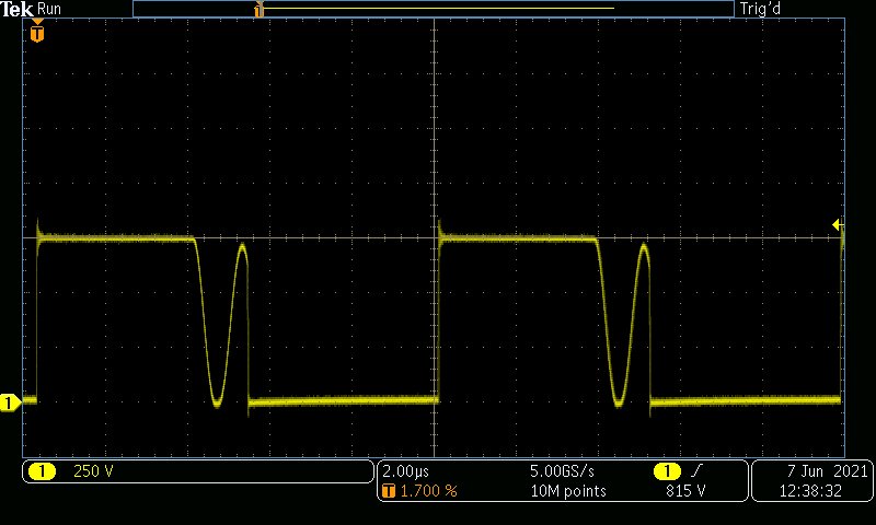 Figure 4-7 VIN = 340 V and VOUT =
400 V at 2 A.
Figure 4-7 VIN = 340 V and VOUT =
400 V at 2 A.Resistive Load (VOUT: 250 V/DIV, 2 µs/DIV, BWL = 800 MHz)
The following figure shows the FET switch node rise time of 22.8 ns at TP7.
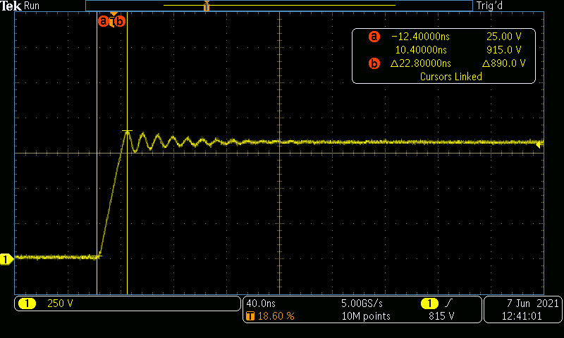 Figure 4-8 VIN = 400 V and VOUT =
400 V at 2 A.
Figure 4-8 VIN = 400 V and VOUT =
400 V at 2 A.Resistive Load (VOUT: 250 V/DIV, 40 ns/DIV, BWL = 800 MHz)