TIDT248A December   2021  – March 2023 TMUXHS4412


  1.   Description
  2.   Features
  3.   Applications
  4. 1Test Prerequisites
    1. 1.1 Voltage and Current Requirements
    2. 1.2 Required Equipment
  5. 2Testing and Results
    1. 2.1 Efficiency Graphs
    2. 2.2 Efficiency Data
    3. 2.3 Thermal Image
    4. 2.4 Dimensions
    5. 2.5 EMI
  6. 3Waveforms
    1. 3.1 Switching
    2. 3.2 Output Voltage Ripple
    3. 3.3 Load Transients
    4. 3.4 Power On and Power Off

Switching

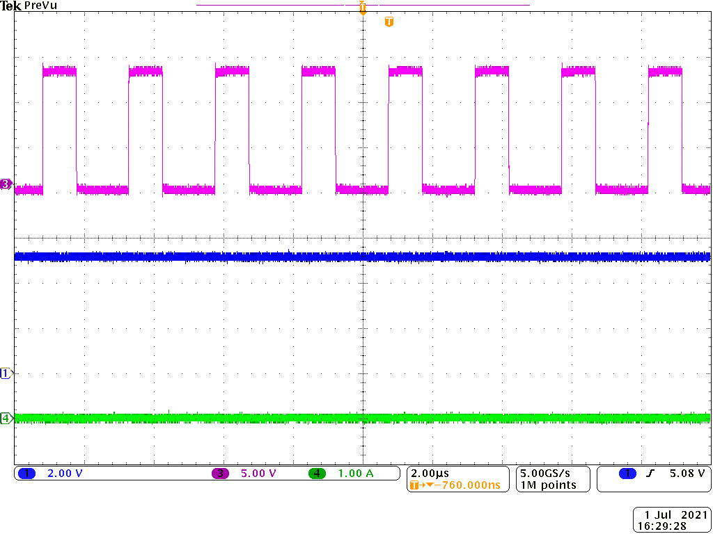
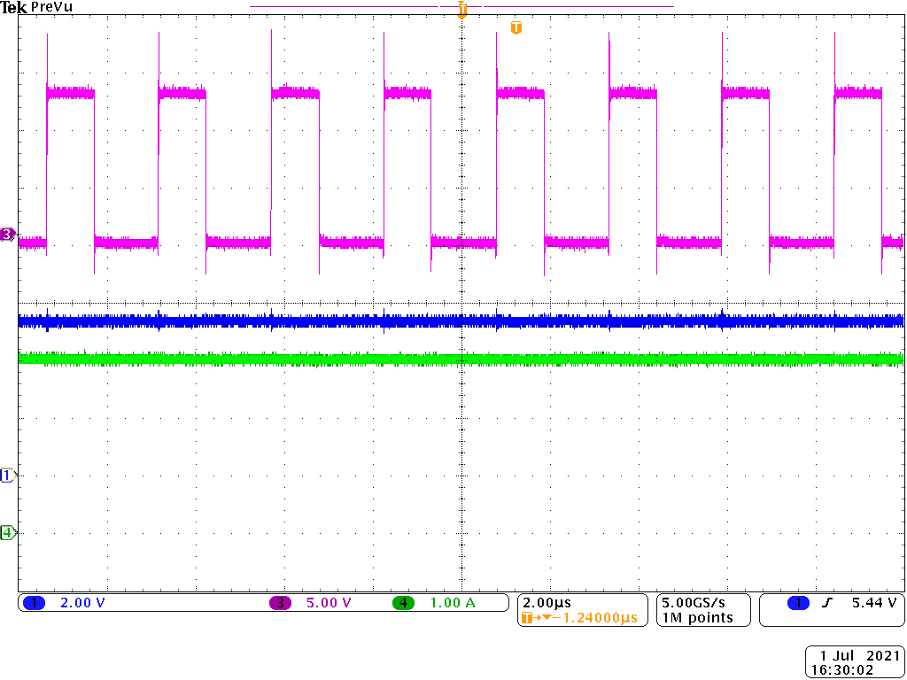
The waveforms of switching nodes at no load and full load condition are shown in following images.
GUID-20211103-SS0I-N0SG-JJCL-PBBJ3QKXSJ8M-low.png
CH1: VPA_BUS, CH3: VSW, CH4: IPA_BUS
Figure 3-1 Switching Waveform, 12-V Input, No Load
GUID-20211103-SS0I-VMP1-KBSR-N4JHCB7PF9MN-low.png
CH1: VPA_BUS, CH3: VSW, CH4: IPA_BUS
Figure 3-2 Switching Waveform, 12-V Input, 3-A Load