TIDT257A February   2022  – October 2022


  1.   Description
  2.   Features
  3.   Application
  4. 1Test Prerequisites
    1. 1.1 Voltage and Current Requirements
    2. 1.2 Considerations
    3. 1.3 Dimensions
  5. 2Testing and Results
    1. 2.1 Efficiency Graphs
    2. 2.2 Efficiency Data
      1. 2.2.1 THD Optimization
    3. 2.3 Thermal Images
      1. 2.3.1 Low-Side GaN Junction Temperature
    4. 2.4 Thermal Mechanical Design
      1. 2.4.1 Design Parameters
      2. 2.4.2 Thermal Resistance Calculation
      3. 2.4.3 Heat-Sink Diagrams
    5. 2.5 EMI
  6. 3Waveforms
    1. 3.1 AC Drop
    2. 3.2 Load Transients
    3. 3.3 Start-Up Sequence

Dimensions

Figure 1-1 illustrates the power supply with a maximum component height of 32 mm (image shown is not to scale).
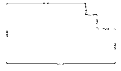
GUID-20220217-SS0I-TQR2-H4QG-45CWPQBTXH96-low.png Figure 1-1 Power-Supply Dimensions

Figure 1-2 shows the FET daughter card dimensions (image shown is not to scale).
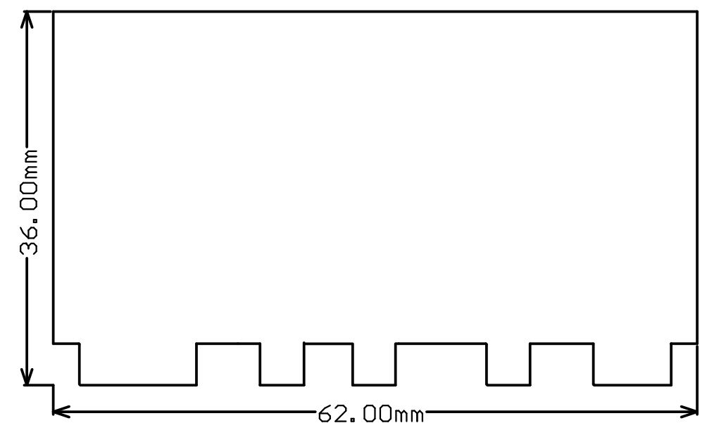
GUID-20221007-SS0I-QLLZ-TK2W-QTCBCXP1KNJ2-low.jpg Figure 1-2 FET Daughter Card Dimensions