TIDT283 May 2022
2.6 Thermal Images
The test conditions for the thermal images are:
24-V input, VDD = 18 V, VEE= –4 V
The load is UCC21732 switching a 0.1-μF capacitive load.
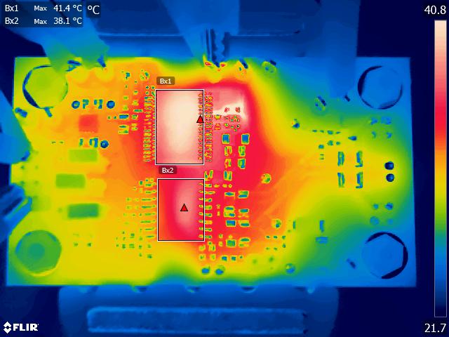
Figure 2-10 shows the thermals while switching a 100-nF load at 1 kHz, which is about 0.18-W power through UCC14240. This is calculated as the sum of the power to charge the gate, and the quiescent power of the gate driver:
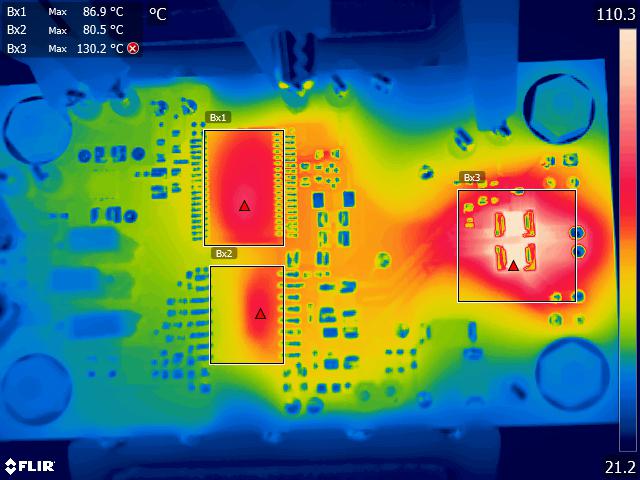
Figure 2-11 shows the thermals while switching a 100-nF load at 35 kHz, which is about 1.5-W power through UCC14240. This is calculated as the sum of the power to charge the gate, and the quiescent power of the gate driver:
The soak time in both cases was 15 minutes, with no forced airflow.
At light load, the UCC14240 temperature peaks at 41.4°C, while the UCC21732 peaks at 38.1°C. The layout of this board balances thermal performance and switch node are. Thermals can be improved by increasing the thermal plane area on the secondary side.
 Figure 2-10 Thermal Image of 100-nF Load
at 1 kHz, 0.17-W Power Draw
Figure 2-10 Thermal Image of 100-nF Load
at 1 kHz, 0.17-W Power DrawAt peak load the UCC14240 temperature peaks at 86.9°C, while the UCC21732 peaks at 80.5°C. The highest temperature on the board is the gate resistors, which is not related to the performance of the ICs, and could be improved by paralleling multiple gate resistors or reducing the gate resistance. The layout of this board balances thermal performance and switch node are. Thermals can be improved by increasing the thermal plane area on the secondary side.
 Figure 2-11 Thermal Image of 100-nF Load
at 35 kHz, 1.5-W Power Draw