TIDT293 October   2022


  1.   Description
  2.   Features
  3.   Applications
  4. 1Design Variants
  5. 2Design Overview
    1. 2.1 Board Contents
    2. 2.2 Connector Description
    3. 2.3 User Interface
      1. 2.3.1 Switches and Push-buttons
      2. 2.3.2 Jumpers
      3. 2.3.3 Potentiometers
    4. 2.4 Functional Block Diagram
    5. 2.5 Functional Block Descriptions
  6. 3Features and Performance Curves
    1. 3.1  Test Setup
    2. 3.2  Pulse
    3. 3.3  Levels and Free Run
    4. 3.4  INP
    5. 3.5  Dual-Output Power Supply
    6. 3.6  Overtemperature Protection
    7. 3.7  Slew Rate Adjust
    8. 3.8  Settling Time Adjust
    9. 3.9  Low- and High-Level Adjust
    10. 3.10 Pulse-Width Adjust
    11. 3.11 Period and Delay Adjust
    12. 3.12 Frequency Response
  7. 4Operation
    1. 4.1 Initial Setup – Jumper Selection and Potentiometer Settings
    2. 4.2 Procedure
      1. 4.2.1 Initial Power Up
      2. 4.2.2 Connecting the Circuit Under Test
  8. 5Limitations and Capabilities
    1. 5.1 Wiring Inductance
    2. 5.2 Minimum Voltage
    3. 5.3 Battery Life
  9. 6Typical Failure Mechanism
    1. 6.1 Fast Thermal Failure
    2. 6.2 Slow Thermal Failure

Low- and High-Level Adjust

The low- and high-level adjustment is made by turning the potentiometers R15 and R23, respectively. Make sure the levels along with the pulse width and period meet the SOA ratings of the FET (Q2).

The following scope plot is a 1-A to 100-A load transient for a 100-V output. The results in the following image use a PSMN035-125B MOSFET in the 100-A, 100-V variant.
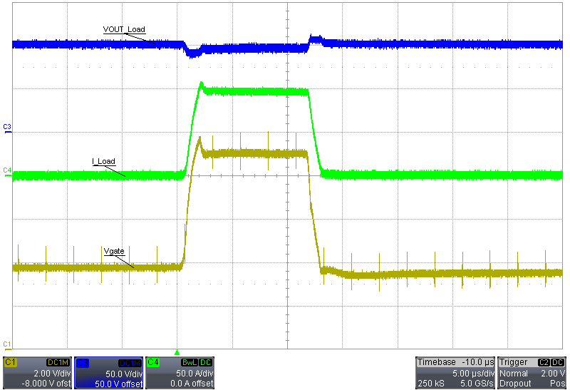
GUID-20220531-SS0I-TFCM-4PW9-MTZ56WC5GQPS-low.pngFigure 3-17 PSMN035-150B 100-V Output, 1-A to 100-A Load Transient

The following scope plot is a 10-A to 25-A load transient for a load of 10 V. The results in the following waveform use a PSMN008-75B MOSFET in the 125-A, 50-V variant.
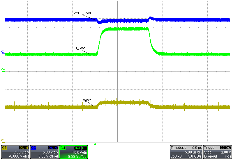
GUID-20220531-SS0I-C3KV-4MCD-0T6BRQBFJPTS-low.pngFigure 3-18 PSMN008-75B, 10-V Output, 10-A to 25-A Load Transient