TIDT293 October   2022


  1.   Description
  2.   Features
  3.   Applications
  4. 1Design Variants
  5. 2Design Overview
    1. 2.1 Board Contents
    2. 2.2 Connector Description
    3. 2.3 User Interface
      1. 2.3.1 Switches and Push-buttons
      2. 2.3.2 Jumpers
      3. 2.3.3 Potentiometers
    4. 2.4 Functional Block Diagram
    5. 2.5 Functional Block Descriptions
  6. 3Features and Performance Curves
    1. 3.1  Test Setup
    2. 3.2  Pulse
    3. 3.3  Levels and Free Run
    4. 3.4  INP
    5. 3.5  Dual-Output Power Supply
    6. 3.6  Overtemperature Protection
    7. 3.7  Slew Rate Adjust
    8. 3.8  Settling Time Adjust
    9. 3.9  Low- and High-Level Adjust
    10. 3.10 Pulse-Width Adjust
    11. 3.11 Period and Delay Adjust
    12. 3.12 Frequency Response
  7. 4Operation
    1. 4.1 Initial Setup – Jumper Selection and Potentiometer Settings
    2. 4.2 Procedure
      1. 4.2.1 Initial Power Up
      2. 4.2.2 Connecting the Circuit Under Test
  8. 5Limitations and Capabilities
    1. 5.1 Wiring Inductance
    2. 5.2 Minimum Voltage
    3. 5.3 Battery Life
  9. 6Typical Failure Mechanism
    1. 6.1 Fast Thermal Failure
    2. 6.2 Slow Thermal Failure

Pulse

When the board is powered, a pulse signal is generated when Pulse (S2) is pushed, or Free run (J6) is installed. Monitor Pulse (TP10) to maintain normal operation. All further scope plots in this user’s guide do trigger on the pulse signal, unless shown otherwise. The following scope plot shows the pulse signal.
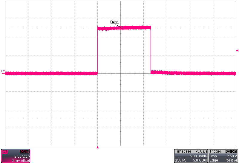
GUID-20220531-SS0I-FGZ6-X4JW-JP34CNCZ7KGJ-low.png Figure 3-5 Measured Pulse Signal From TP10